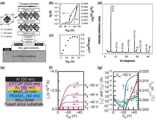
Figure 19.

2D (PEA)2SnI4‐based FETs. a) Schematic illustration of a BGBC FET structure with a layered (PEA)2SnI4 channel. b) Corresponding transfer characteristics at V D = −100 V. c) Corresponding extracted hole mobility. d) XRD spectrum of a layered (PEA)2SnI4 thin film. a–d) Reproduced with permission.[ 240 ] Copyright 1999, American Association for the Advancement of Science. e) Schematic representation of a TGTC FET structure with (PEA)2SnI4 semiconducting channel, SAM‐treated substrate, and MoO x hole‐injection layer. f) Corresponding FET output curves. g) Corresponding transfer characteristics. e–g) Reproduced with permission.[ 238 ] Copyright 2016, Wiley‐VCH.
