Figure 21.

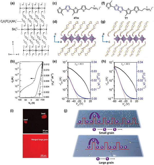
2D organic spacer synthesis and FET fabrication. a) (4‐FPEA)2SnI4 crystal structure, viewed along the (011) axis. b) Corresponding BGBC FET transfer characteristics. a,b) Reproduced with permission.[ 27 ] Copyright 2001, American Chemical Society. c) Chemical structure of 4Tm. d) Side‐view of (4Tm)2SnI4 crystal structure. e) Corresponding FET transfer characteristics. f) Chemical structure of TT. g) Side‐view of (TT)2SnI4 crystal structure. h) Corresponding FET transfer characteristics. i) PL images of (TT)2SnI4 thin films after thermal annealing treatment at 155°C for 4 min (top) and 15 min (bottom) (scale bar = 20 µm). j) Schematic representation of carrier transport in small grain (top) and large grain (bottom)‐based (TT)2SnI4 thin film. c–j) Reproduced with permission.[ 259 ] Copyright 2021, American Chemical Society.
