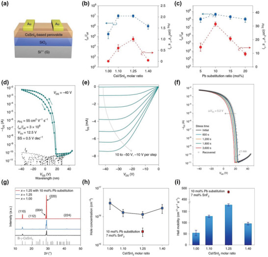
Figure 23.

3D CsSnI3‐based FET. a) Schematic illustration of BGTC TFT structure. b) µ FE and I on/I off of CsSnI3‐based TFTs with different molar ratios of CsI/SnI2. c) µ FE and I on/I off of CsI‐rich (x = 1.25) precursors with various ratios of Pb substitution. d) Transfer characteristics of optimized CsSnI3‐based TFT (x = 1.25, 10 mol% Pb substitution, and 7 mol% of SnF2). e) Corresponding output curves. f) Transfer curves of one optimized CsSnI3‐based TFT under negative bias–stress measurement for various durations and the recovery behavior at V GS = V DS = −40 V. g) XRD patterns of perovskite films deposited from precursors with different ratios of CsI/SnI2 and that from CsI‐rich (x = 1.25) precursor with 10 mol% Pb substitution and 7 mol% SnF2. Hall measurement derived parameters, including h) hole concentration of thin films deposited from precursors with different CsI/SnI2 ratios (without SnF2) and that from optimized CsI‐rich (x = 1.25), 10 mol% Pb substitution, and 7 mol% SnF2 precursor and i) corresponding Hall mobility. a–i) Reproduced with permission.[ 20 ] Copyright 2022, Nature Publishing Group.
