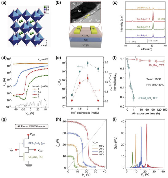
Figure 25.

Sn2+‐free perovskite FET. a) The crystal lattice structure of vacancy‐ordered double perovskite Cs2SnI6. b) TFT structure and corresponding cross‐sectional TEM image. c) X‐ray diffraction peak patterns of Cs2SnI6 as a function of the CsI:SnI4 ratio in the precursor solution. d) Transfer characteristics of Cs2SnI6 TFT with various ratios of Mn2+ doping. e) Summary of electron mobility µ e and I on/I off of TFTs. f) Normalized µ FE of Sn2+‐based (PEA)2SnI4 TFT and Sn(IV)‐based Cs2SnI6 TFTs as a function of ambient air exposure time. g) Schematic diagram of CMOS inverter with combined p‐channel (PEA)2SnI4 TFT and n‐channel Mn2+‐doped Cs2SnI6 TFT. Corresponding h) voltage transfer and i) gain voltage curves at different V DDs. a–i) Reproduced with permission.[ 92 ] Copyright 2022, Cell Press.
