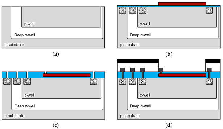
Figure 4.
Cross-sectional schematic of the sensor fabrication process. (a) A p-type 4-in silicon wafer (60 Ω/cm) is ion-implanted and driven in under the conditions that are shown in Table 1 to form a double-diffusion well structure; (b) the gate oxide film of 60 nm and Poly-Si of 350 nm are deposited, and the gate electrode is formed by phosphorous diffusion; (c) 400-nm-thick Tetra ethoxy silane (TEOS) is deposited by low-pressure chemical vapor deposition (LP-CVD), and contact holes are opened by oxide film etching; (d) after Al wiring, a light shielding film is formed by Al sputtering of 1.0 µm outside the sensing area.

