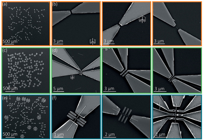
Figure 3.
SEM image showing automatically fabricated (a) source and drain contacts with (b) higher magnification examples showing accurate alignment to the nanowire, (c) four-point contact with (d) higher magnification examples, and (e) double-quantum-dot gate with (f) higher magnification examples of nanowire devices on separate areas of a chip, each on a 2 × 2 mm2 area.

