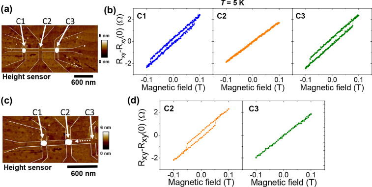
Figure 4.
(a) Tapping mode AFM image of the nano-Hall bar structure with two C50 MNPs placed above devices C1 and C3. (b) Hall resistance Rxy as a function of perpendicular magnetic field. (c) Tapping mode AFM image of the same nano-Hall bar structure after one of the C50 MNPs was moved from device C3 to C2 by the AFM tip. (d) Hall resistance Rxy as a function of perpendicular magnetic field after movement of the MNP from C3 to C2. All electrical transport measurements were performed at T = 5 K using a bias current of 1 μA.

