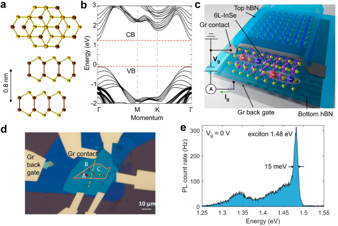
Figure 1.
Few-layer InSe in a field-effect device structure. (a) Top and side views of γ-stacked bilayer InSe. Brown spheres, indium atoms; yellow spheres, selenium atoms. The interlayer distance is about 0.8 nm. (b) Calculated band diagram for six-layer InSe (6L-InSe). CB, conduction band; VB, valence band. (c) Schematic of the hBN-encapsulated 6L-InSe device (device A) with a few-layer graphene contact and bottom gate. (d) Optical microscope image of device A. The orange contour encloses the region of the InSe flake. The dashed line indicates the position of the few-layer graphene contact on the flake. Scale bar, 10 μm. (e) PL count rate as a function of the emission energy at Vg = 0 V using P = 50 μW, measured at position A in (d).

