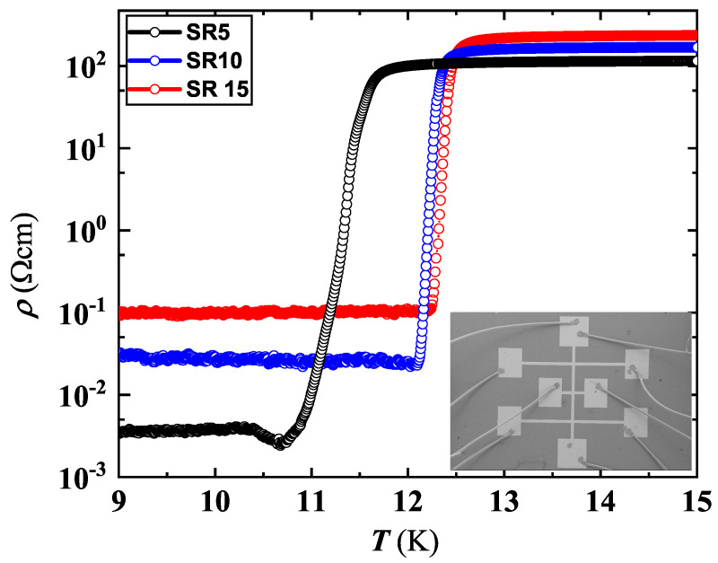
Figure 1.
NbN resistivity behavior around , for the set deposited on the AlO r−cut substrate (see Table 1). Inset: Scanning electron microscopy of a typical Hall bar shaped film with Al wires bonded to sample pads. Current carrying contacts were located on the top and bottom, along the vertical line; and a couple of lateral contacts from the same side were used to detect the voltage drop.

