Abstract
Silicon photonic platforms offer relevance to large markets in many applications, such as optical phased arrays, photonic neural networks, programmable photonic integrated circuits, and quantum computation devices. As one of the basic tuning devices, the thermo-optic phase shifter (TOPS) plays an important role in all these applications. A TOPS with the merits of easy fabrication, low power consumption, small thermal time constant, low insertion loss, small footprint, and low crosstalk, is needed to improve the performance and lower the cost of the above applications. To meet these demands, various TOPS have been proposed and experimentally demonstrated on different foundry platforms In this paper, we review the state-of-the-art of TOPS, including metal heater, doped silicon, silicide, with silicon substrate undercut for heat insulation, folded waveguide structure, and multi-pass waveguide structure. We further compare these TOPSs and propose the directions of the future developments on TOPS.
Graphical abstract
Keywords: Thermo-optic phase shifter, Photonic integrated circuits (PICs), Optical switches, Silicon photonics
Introduction
Benefiting from the complementary metal–oxide–semiconductor (CMOS) compatibility, silicon photonics is becoming a key technology for implementing high-density photonic integrated circuits (PICs) with complex functionalities [1–3]. The functions of these PICs are usually achieved through phase shifters [4, 5]. Tuning principles of phase shifters are mainly based on the thermo-optic effect, the electro-optic effect, or the nano-opto-electro-mechanical effect [6–8]. Some other types of phase shifters have also been proposed and used extensively [9, 10]. The thermo-optic coefficient of silicon in the C band over the temperature range 300–600 K can be written as [11]
Therefore, the refractive index of a waveguide can be changed through a thermo-optic phase shifter (TOPS). The values of thermo-optic coefficient and heat conductivity are about 1.8 × 10⁻⁴ K–1 and 149 W/mK, respectively [12]. Compared with the TOPS, electro-optic phase shifters always have a greater modulation bandwidth due to the free-carrier plasma dispersion effect. However, these devices usually suffer from substantial insertion loss due to free-carrier absorption [13]. Although the phase shifter based on the nano-opto-electro-mechanical effect has low power consumption, it is hard to fabricate. In addition, this type of phase shifter is liable to break down due to mechanical fatigue [14].
As a result of simple design, easy fabrication, low cost, and small footprint, the TOPS is widely used for photonic devices and large-scale integrated PICs on the silicon-on-insulator (SOI) platform [15–17]. Typical photonic devices that use the TOPS are Mach–Zehnder interferometer (MZI) [18–20], micro-disk [21], and micro-ring resonator (MRR) [22–24]. The TOPS in these photonic devices is used to change the phase of light by locally controlling the temperature in the phase-shifting region with TOPS. However, it is worth mentioning that the modulation bandwidth of TOPS is less than one hundred of kilohertz, the TOPS is only suitable for applications that do not require high modulation speed [25–28]. Regarding these characteristics of TOPS, monolithic integrated PIC with TOPS have been applied in some special applications, such as optical neural networks [29–31], quantum photonic devices [32–34], optical phased array [35, 36], reconfigurable optical add-drop multiplexers (ROADMs) [37], programmable photonic circuit [38–40], and thermally-tunable optical delay lines [41]. The requirements of these PICs for TOPS will be discussed in Sect. 4.
Many researchers are working toward improving the performance of TOPS [42–45]. Methods including air-gap trench or silicon substrate undercut post-processing, folded waveguide, and multi-pass waveguide have been proposed and demonstrated. A trade-off between the power consumption and the thermal time constant has also been investigated [46, 47]. In this paper, we give an overview of the current status of the TOPS based on silicon photonics technologies. More specifically, we focus on the TOPS that is ready for massive application and fabricated in foundry platforms, including IMEC, AMF, IBM, OpSIS, CUMEC, and so on, by a standard silicon fabrication process, We also discuss the outlook for further development of TOPS, at the end of this paper.
Principle of TOPS
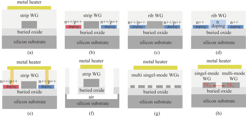
A TOPS is composed of a waveguide structure and a resistive heater. As shown in Fig. 1a and c, the shape of a waveguide on the SOI platform can be a strip or rib structure. Typically, both of them consist of a 2.0 μm silica lower cladding, 220 nm silicon core, and 2.0 μm silica upper cladding. Figure 1a–h provides the cross-sections of different kinds of TOPS, which will be discussed in detail in Sect. 3.
Fig. 1.
Cross-sections of different kinds of TOPS. a TOPS based on strip waveguide with a metal heater on the top. b TOPS based on strip waveguide with doped-silicon heaters at both sides. c TOPS based on rib waveguide with doped-silicon heaters at both sides. d TOPS based on rib waveguide with a directly integrated doped silicon heater. e TOPS based on strip waveguide surrounded by a hybrid heater. f TOPS with air-gap trench and silicon substrate undercut. g TOPS based on the folded waveguide with a metal heater on the top. h TOPS based on multi-pass waveguides with a metal heater on the top
Due to the wide variety of materials and design complexities offered by CMOS technologies, the material used for the resistive heater can be doped silicon, silicide, or metal wiring. The line resistivity and fabrication process of the three types of heaters are different, which makes it possible to design heaters with different dimensions.
Generally, the amount of phase shift caused by resistive heater can be expressed as [48]
| 1 |
where λ is the wavelength of the light, is the thermo-optic coefficient of the silicon waveguide, L is the length of TOPS, and ΔT denotes the change of temperature. Since ΔT is caused by the action of the resistive heater, it can be written as
| 2 |
Here, η is the utilization tuning efficiency of drive power, P is the power consumed by the resistive heater, Cp is the heat capacity of the waveguide, ρ is the material density of the waveguide, and S is the cross-sectional area of the waveguide. The amount of phase shift can be written as
| 3 |
The tuning efficiency of TOPS is usually expressed in terms of electrical power needed for a π phase shift (Pπ), which can be expressed as
| 4 |
Therefore, the tuning efficiency of TOPS is mainly determined by the utilization tuning efficiency of drive power. An effective way to improve the tuning efficiency of TOPS is reducing heat leakage to the environment.
In addition to tuning efficiency, the thermal time constant is also an important factor for TOPS. The thermal thermal time constant of TOPS can be written as
| 5 |
where H is the heat capacity of the heated waveguide, and G denotes the thermal conductance of the waveguide to the environment. H and G can be expressed as
| 6 |
Here, A is the area of heat flow. By substituting Eqs. (2) and (6) into Eq. (5), the thermal time constant can be rewritten as
| 7 |
Therefore, the thermal time constant is influenced by the utilization efficiency, the area perpendicular to the direction of heat flow, and the cross-sectional area of the waveguide. Moreover, the product of thermal time constant and power consumption, i.e., the figure of merit (FOM), can be expressed as
| 8 |
which can be reduced by decreasing the area perpendicular to the direction of heat flow, such as by directly integrating a doped silicon heater with a waveguide. However, the insertion loss of this kind of TOPS is relatively large, which is not suitable for large-scale networks. In addition, the TOPSs with folded and multi-pass waveguide have been proposed to reduce power consumption. Adversely, this type of structure would increase the size of the footprint and insertion loss. The pros and cons of all these TOPS devices will be described in the next section.
Comparison of different TOPS
Many studies have focused on improving the characteristics of TOPS, such as by increased tuning efficiency, faster thermal time constant, lower insertion loss, and smaller footprint. According to the difference between the structural differences of these TOPSs they can be classified as a basic structure, silicon substrate undercut, folded waveguide, multi-pass waveguide, and integrated with diode.
TOPS with a basic structure
For a basic TOPS structure, a resistive heater of doped silicon or silicide is placed on both sides of a waveguide. At the same time, a metal resistive heater can be fabricated above the waveguide, as shown in Fig. 2. It needs to be mentioned that the resistivity of the heater line should be much larger than that of connecting wire, which is usually made of metal aluminum (Al) or copper (Cu).
Fig. 2.
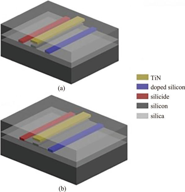
Different TOPS of a strip waveguide and b rib waveguide with a basic structure based on SOI platform
Almost all silicon foundry platforms can manufacture these types of TOPSs, whose performances are shown in Table 1. The columns include heater type, waveguide type, test structure, tuning efficiency, heating time, cooling time, and foundry.
Table 1.
Performance list of conventional TOPS fabricated on different foundries
| Heater type | Waveguide type | Test structure | Tuning efficiency/(mW·π–1) | Heating time/μs | Cooling time/μs | Foundry | References |
|---|---|---|---|---|---|---|---|
| TiN | Single strip WG | MZI | 19.12 | 5.90 | 8.97 | CUMEC | [49] |
| Silicide | Single strip WG | MZI | 21.75 | 12.90 | 4.0 | CUMEC | [49] |
| Doped silicon | Single strip WG | MZI | 21.96 | 12.80 | 2.60 | CUMEC | [49] |
| Tungsten | Single strip WG | MZI | 23.4 | 38.2 | 45.11 | IMEC | [50] |
| Silicide | Single strip WG | MZI | 22.5 | 19.1 | 75.8 | IMEC | [50] |
| Doped silicon | Single strip WG | MZI | 20.4 | 21.3 | 66.0 | IMEC | [50] |
| TiN | Single strip WG | MZI | 21.4 | 5.6 | NR | AMF | [15] |
| Silicide | Single rib WG | MZI | 20 | 2.8 | 2.2 | IBM | [16] |
| Doped silicon | Single rib WG | MZI | 24.77 ± 0.43 | NR | NR | OpSIS | [51] |
TiN: titanium nitride, WG: waveguide, NR: not reported, MZI: Mach–Zehnder interferometer
The tuning efficiency of all these TOPS with a basic structure is about 20 mW/π. The minor differences among tuning efficiency and thermal time constant of these TOPS might be caused by the material characteristics, processing technology, and testing equipment. The characteristics of these TOPS fabricated on CUMEC and other foundries are on the same level.
Moreover, the drive voltage of TOPS can be written as [16]
| 9 |
Here, P is the drive power of TOPS, and R denotes the resistance of the heater in TOPS. To use CMOS compatible drive voltage, which is always less than 1.0 V, a heater of silicide elements is electrically connected in parallel utilizing Cu connections (see Fig. 3). The resistance can be small enough, using the parallel connection, to apply a low drive voltage [16]. As a result, this kind of TOPS operates with the tuning efficiency of Pπ = 20 mW/π and a thermal time constant of τ < 2.8 μs, using a 1 V drive voltage. Unfortunately, the excess optical loss is about 25 dB/cm, which is caused by scattering and absorption loss [16].
Fig. 3.
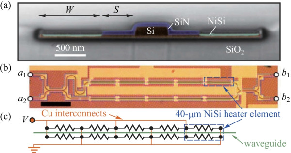
TOPS with an electrically parallel heater [16]. a Scanning electron micrograph (SEM) cross-sectional image of an SOI rib waveguide with a heater of silicide. b Heater of silicide was implemented into the MZI. c Electrical configuration of the heater of silicide in the upper arm of the MZI
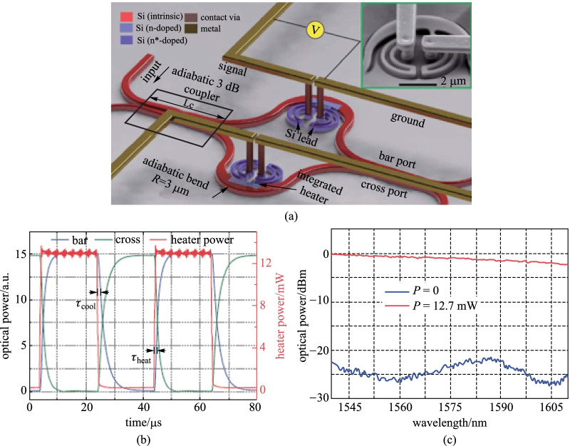
In addition, a TOPS based on a strip waveguide with a directly integrated doped silicon heater has been demonstrated by Watts et al. [48], as shown in Fig. 4. Although the thermal time constant is the same as the TOPS with an electrically parallel heater, the tuning efficiency is only 12.7 mW/π due to the silicon waveguide core itself being used as a resistive heater. The insertion loss of the TOPS with a directly integrated doped silicon heater is about 0.5 dB, which is not beneficial for a large-scale PIC.
Fig. 4.
TOPS with a directly integrated silicon heater [48]. a Schematics of the proposed structure. Inset: SEM image of the fabricated optical switch. b Time-domain measurement of the fabricated TOPS under an electrical consumption power of 12.7 mW, with a heating time and cooling time of 2.2 and 2.4 μs, separately. c Frequency domain measurement in the cross port showing a bandwidth of 70 nm and extinction of > 20 dB
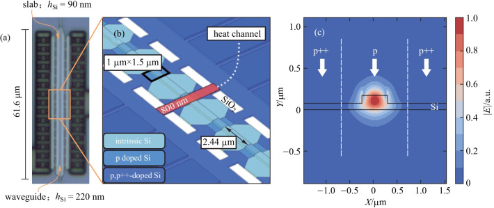
Due to the fact that insertion loss of a TOPS with a directly doped silicon heater in Ref. [48] is high, a novel TOPS with low-loss has been proposed and experimentally proved by Harris et al. [51]. As shown in Fig. 5b, there is only an 800 nm wide channel connecting the contact region to the ridge waveguide, which efficiently restricts the outward propagation of heat. There is sufficient clearance between the guiding region and the p++-doped region of 2.44 μm to avoide insertion loss due to the free-carrier absorption. A 61.6 μm long TOPS is fabricated with a propagation loss of (0.23 ± 0.13) dB for 21 devices. At the same time, the Pπ of the device is (24.77 ± 0.43) mW/π and the thermal time constant of the device is 2.69 μs, which is similar to the results of TOPS in Refs. [16, 48].
Fig. 5.
A low-loss TOPS with a directly integrated silicon heater [51]. a Optical micrograph of the structure. b Perspective view of the structure. c Doping profile along the cross-section marked red in (b), overlapped with the simulated amplitude of the horizontal component of the electrical field
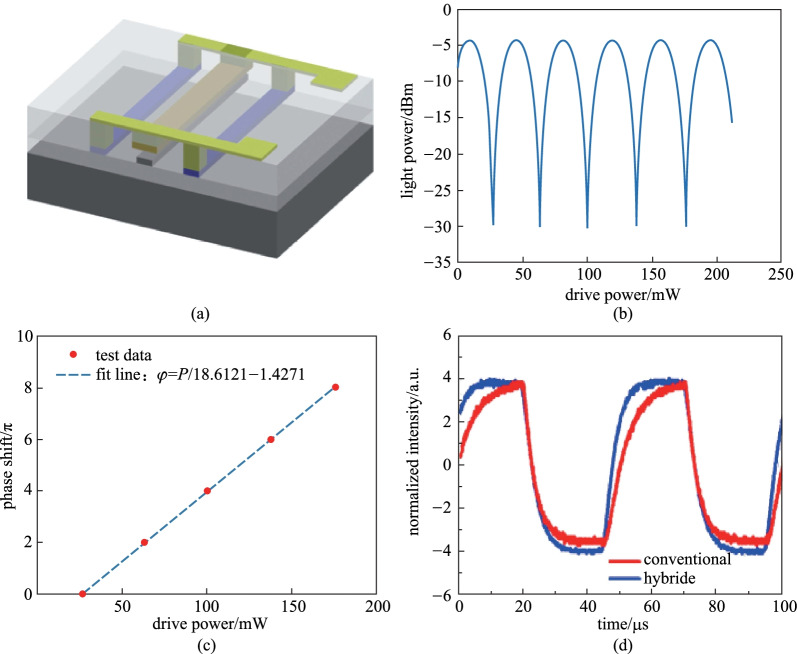
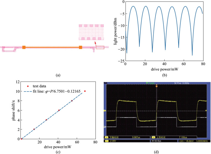
Furthermore, we proposed a hybrid TOPS and fabricated it on the CUMEC silicon foundry platform, as shown in Fig. 6a. Figure 6b is the curve of output power versus the drive power when the TOPS is placed on one arm of the MZI structure. Figure 6c shows the fitting line of the variation of phase shift versus the drive power. The slope of the fitting line denotes the tuning efficiency, which is about 18.61 mW/π. As shown in Fig. 6d, the thermal time constant of TOPS with a hybrid structure is much smaller than the TOPS with a basic structure, without sacrificing tuning efficiency.
Fig. 6.
A hybrid TOPS. a Schematic of the hybrid TOPS. b Output light power versus the drive power. c Variation of phase shift versus the drive power. d Response time curve of TOPS with the basic structure and hybrid structure
TOPS with the silicon substrate undercut
The thermal conductivity of air, at 0.31 W/(m·K), is almost three orders of magnitude smaller than that of silicon, 150 W/(m·K). An air-gap trench and silicon substrate undercut post-processing have been chosen to reduce the heat leakage to the environment, as shown in Fig. 7. Table 2 is the experimental results for TOPS devices with silicon substrate undercut which have been designed and fabricated by different organizations. As compared to the TOPS with the basic structure, a significant improvement of tuning efficiency is achieved. However, the thermal time constant is adversely affected due to the reduced heat conductivity by the air-gap trench and silicon substrate undercut. When a TOPS with silicon substrate undercut is applied in one phase arm of the MZI structure the thermal time constant is no less than 266 μs [50, 52–54]. The relationship between thermal time constant and − 3 dB bandwidth (f−3 dB) [55, 56] can be written as
| 10 |
Fig. 7.
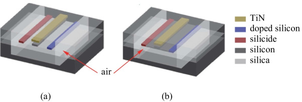
Schematic of TOPS of a strip waveguide and b rib waveguide with air-gap trench and silicon substrate undercut
Table 2.
Performance list of TOPS with silicon substrate undercut designed and fabricated by different organizations
| Heater type | Waveguide type | Test structure | Tuning efficiency/(mW·π–1) | Heating time/μs | Cooling time/μs | Organization | References |
|---|---|---|---|---|---|---|---|
| Tungsten | Single strip WG | MZI | 1.42 | 198 | 227 | IMEC | [50] |
| Silicide | Single strip WG | MZI | 1.49 | 188 | 218 | IMEC | [50] |
| Doped silicon | Single strip WG | MZI | 1.42 | 151 | 217 | IMEC | [50] |
| TiN | Single strip WG | MZI | 0.49 | 144 | 122 | IME | [52] |
| TiN | Single strip WG | MI | 0.05 | 780 | 500 | IME | [53] |
| Pt | Single strip WG | MZI | 0.54 | 141 | NR | OSU | [54] |
| TiN | Threefolded strip WG | MZI | 0.5 | 640 | 700 | Huawei | [57] |
| TiN | 9-folded strip WG | MZI | 0.095 | 750 | 1200 | UBC | [58] |
TiN: titanium nitride, WG: waveguide, NR: not reported, MZI: Mach–Zehnder interferometer, MI: Michelson interferometer
Therefore, the − 3 dB bandwidth of TOPS with air-gap trench and silicon substrate undercut is below 2.6 kHz, which makes them unattractive for several emerging applications.
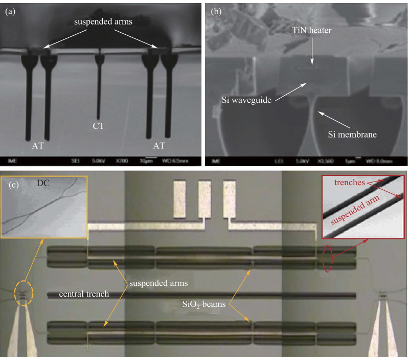
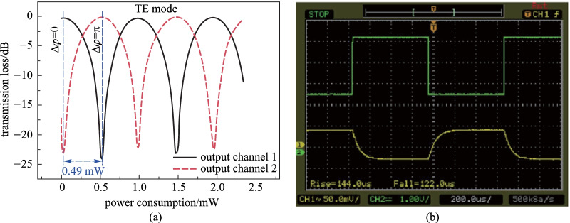
Except for the structure in Ref. [54], all the other structures shown in Table 2 are fabricated on the SOI platform. After a standard back-end process, an air-gap trench was fabricated by deep-etching down to the silicon substrate. Then, anisotropic selective silicon etching was applied to the silicon substrate to undercut the waveguides [52]. Perspective and cross-section images are shown in Fig. 8. Here, two 4.0 μm wide arm trenches are fabricated on both sides of each TOPS to prevent the heat from leaking into the adjacent SiO2 layer. Another central trench is designed at the center of the two arms to further reduce the thermal crosstalk. The transmission loss of the switch for TE mode at 1550 nm as a function of power consumption and the time-domain response characteristics are shown in Fig. 9. The optical crosstalk of this switch is more than 23 dB, and the switching power, i.e., tuning efficiency of TOPS, is only 0.49 mW/π. The 10%–90% thermal time constant is about 266 μs, including the rise time of 144 μs and the fall time of 122 μs.
Fig. 8.
SEM images of TOPS with suspended arms [52]. a Cross-sectional SEM images (AT: arm trenches, CT: central trench). b Cross-section of the suspended arm. c Schematic diagram of 2 × 2 silicon photonics switch with suspended phase arms
Fig. 9.
Experimental results. (a) Tuning efficiency curve and (b) rise time and drop time of TOPS with suspended arms [52]
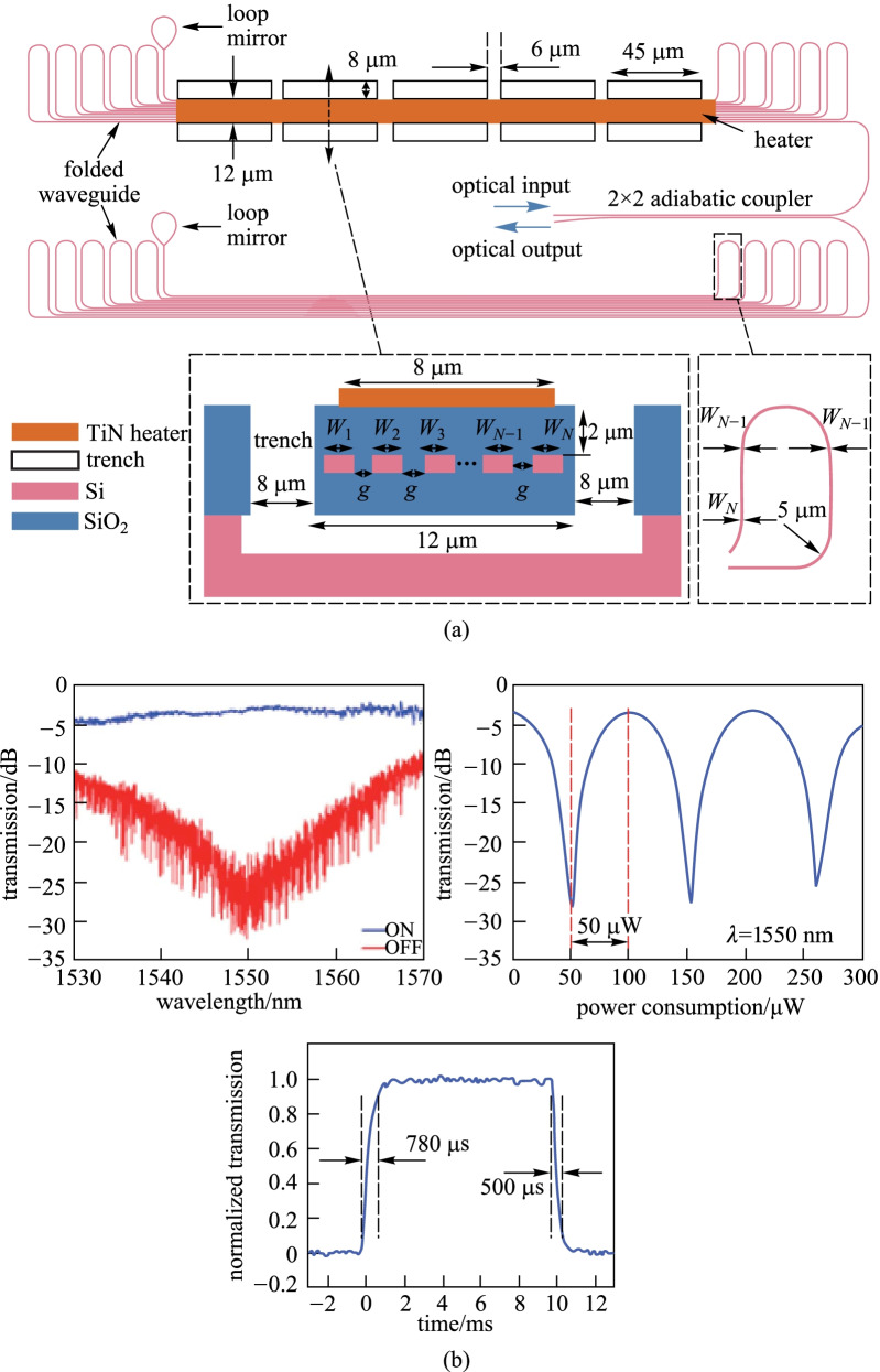
To further improve the tuning efficiency of the TOPS, a folded waveguide and suspended structure have been adopted simultaneously [53], as shown in Fig. 10a. The two types of structures are used to increase the optical interaction length of the light with the heated region and improve thermal isolation, respectively. Finally, the tuning efficiency can be improved to 0.05 mW/π, which is an order of magnitude higher than the TOPS with silicon substrate undercut reported in other literature [50, 54, 57, 58]. Here, a Michelson interferometer (MI) has been adopted to replace the MZI [57]. The measurement results have been shown in Fig. 10b, the measured power required to switch from the maximum to minimum transmission is only 50 μW, and the thermal time constant is 1.28 ms, including a rise time of 780 μs and fall time of 500 μs.
Fig. 10.
Schematic and experimental results of Michelson interferometer [57]. a Schematic of Michelson interferometer based on the TOPS with folded waveguides and suspended structure. b Measurement results for the device
The process of producing silicon substrate undercut is much more complex than that of producing the basic structure, and this kind of TOPS on our silicon platform is still under development. At the same time, the temperature variation of waveguides versus different structures has been analyzed. As shown in Fig. 11, the temperature variation of the waveguide of TOPS with silicon substrate undercut is much larger than the TOPS with only an air-gap trench and basic structure, which means the tuning efficiency of TOPS with undercut is much higher than the TOPS with only an air-gap trench.
Fig. 11.
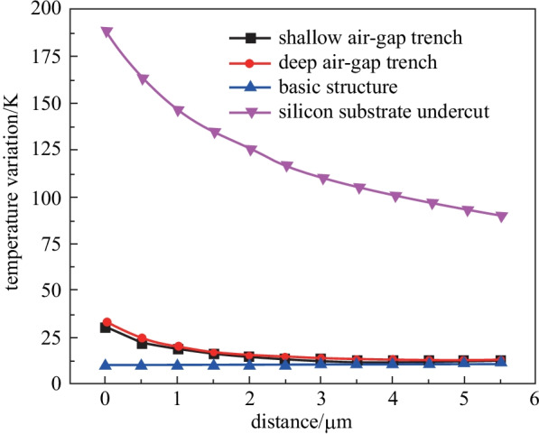
Simulation results of the temperature variation of the waveguide along with the distance between the waveguide and air-gap trench
Although the tuning efficiency of TOPS can be improved by creating a vertical air-gap trench and silicon substrate undercut surrounding the silicon waveguide [50, 52–54, 57, 58], some drawbacks have also been caused. First, densely placed air-gap trenches or silicon substrate undercut structures over a large area limits the scalability of integration. Second, the reliability has been reduced due to the accumulated mechanical fatigue from temperature stress. Third, the thermal time constant has increased by about 20 times. Therefore, the TOPS with air-gap trench and silicon substrate undercut is unbeneficial for applications that require fast response, such as optical neural networks, quantum computation devices [15].
TOPS with a folded waveguide
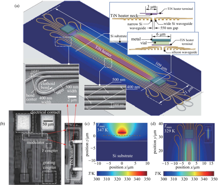
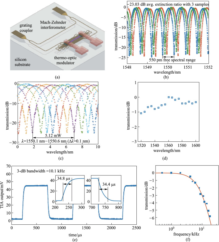
Due to the fact that the area of heat flow is much larger than the cross-section area of the waveguide, TOPS devices with folded waveguides have been proposed and fabricated [57–59]. Recently, Chung et al. have reported an experimental demonstration of geometrical design optimization for improving the tuning efficiency of a low-loss silicon thermo-optic waveguide phase shifter on a standard silicon photonics platform (see Fig. 12) [59], whose footprint is only 0.0023 mm2. The TOPS has been experimentally measured using an on-chip MZI, and the results are shown in Fig. 13. The TOPS consumes 2.56 mW for a π phase shift over 100 nm optical bandwidth while achieving 1.23 dB optical loss. Besides, the − 3 dB bandwidth of the TOPS is about 10.1 kHz. Therefore, the Pπ·τ product of the TOPS is about 88.57 mW/π·μs.
Fig. 12.
Fabricated structure of a TOPS with geometrical design optimization for tuning efficiency improvement [59]. a Physical layout of the fabricated TOPS with SEM photographs of multi-section Clothoid bend structures and waveguide array with alternating widths. b Microphotograph of a fabricated TOPS test chip. c Vertical and d horizontal cross-section of the TOPS with simulated temperature profile at the center of the silicon waveguide
Fig. 13.
Experimental results of TOPS with the folded waveguide [59]. a MZI structure for a test. b Spectral of three samples with average extinction ratio –23.03 dB. c Tuning efficiency of 2.56 mW/π. d Normalized optical transmission. e Rise time and fall time of 34.8 and 34.4 μs. f Thermo-optic bandwidth test
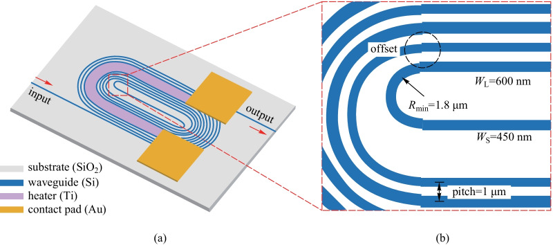
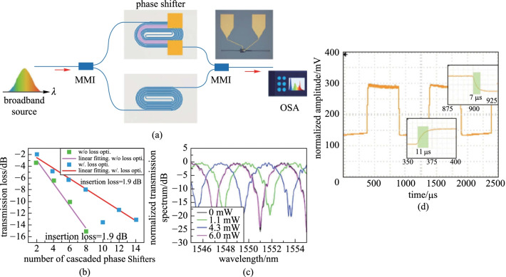
In addition, a TOPS based on a densely distributed silicon spiral waveguide on an SOI platform has been experimentally demonstrated by Qiu et al. [60] (see Fig. 14). The phase shifter shows a well-balanced performance in all aspects. The electric power consumption is as low as 3 mW to achieve a phase shift, the optical insertion loss is 0.9 dB, the footprint is 67 × 28 μm2 under a standard silicon photonics fabrication process without silicon air-gap trench or substrate undercut process, and the modulation bandwidth is measured to be 39 kHz, as shown in Fig. 15.
Fig. 14.
a Schematic of the proposed TOPS using a spiral waveguide. b Zoom-in the offset part [60]
Fig. 15.
a MZI structure for measuring the phase tuning tuning efficiency. b Insertion loss of the device with optimization. c Spectrum of the MZI with the electrical power varies from 0 to 6.0 mW. d Modulation bandwidth of the TOPS [60]
The FOM of the TOPS is about 33 mW/π·μs, which is a benefit for large-scale silicon PICs as an efficient fundamental unit. Compared with the TOPS with silicon substrate undercut, this kind of structure is much easier to fabricate with a lower FOM value. Besides, the tuning efficiency of this kind of TOPS can be adjusted by changing the folded times of the waveguide. Unfortunately, the insertion loss is positively related to the folded times of the waveguide.
To obtain the optimal folded times of waveguide, we have fabricated TOPS devices with folded waveguide on the CUMEC silicon platform and have analyzed their performances in terms of a new figure of merit (FOM2), accounting for the influence of the insertion loss:
| 11 |
where IL is the insertion loss of the device. As shown in Fig. 16, the widths of the two adjacent waveguides are 450 and 500 nm. The two waveguides are interval distribution with a spacing of 554 nm. There is no mode crosstalk between the two adjacent waveguides because the effective indices of the two waveguides are different. The propagation loss of the bend can be ignored since the radius is much larger than 5.0 μm. The heater is TiN metal and placed on top of the waveguide.
Fig. 16.
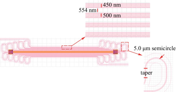
Schematic of TOPS with a folded waveguide fabricated on CUMEC silicon platform
The loss of the device is only determined by the length of the folded waveguide. Therefore, Eq. (11) can be wrn as
| 12 |
Here, ILs and n are the loss of single folded waveguide and the folded times of waveguide, respectively. As shown in Fig. 17c, when the folded time of the waveguide is 2, the FOM2 is smallest. Consideration of the actual layout, a TOPS composed of a threefolded waveguide is a benefit for a large-scale PIC. Figure 17a and b is the curve of the tuning efficiency and thermal time constant versus the number of folds of the waveguide.
Fig. 17.
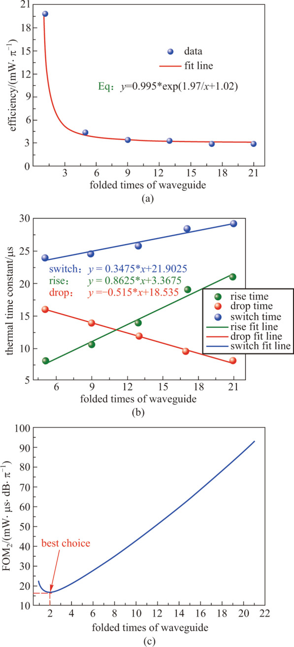
Experimental results of TOPS with folded waveguides, a tuning efficiency, b thermal time constant, c value of FOM2 versus with different folded times of waveguide
TOPS with a multi-pass waveguide
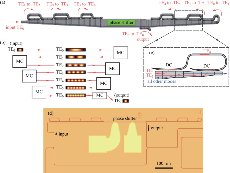
As is well known, there is always a trade-off between the tuning efficiency and thermal time constant of TOPS. To improve the tuning efficiency of TOPS without sacrificing the thermal time constant, light recycling based on resonators has been employed to improve the utilization tuning efficiency of drive power. As shown in Fig. 18, a multi-pass TOPS that lowers power consumption to 1.7 mW per π phase shift has been experimentally demonstrated [43]. The heater is placed on the top of the waveguide. An tuning efficiency of 15.4, 4.6, 2.6, and 1.7 mW/π are measured in the 1-pass, 3-pass, 5-pass, and 7-pass phase shifter, respectively. This corresponds to a power-tuning efficiency enhancement of 3.3, 5.9, and 8.9 times in the 3-pass, 5-pass, and 7-pass phase shifter, respectively. Note that the factor of enhancement is slightly higher than the number of passes. This is because the effective refractive indices of the higher-order modes are more sensitive to temperature change due to stronger dispersion. A thermal time constant of 6.5 μs is measured, which is independent of the number of passes, as shown in Fig. 19.
Fig. 18.
Multi-pass TOPS based on mode multiplexing [61]. a Schematic of a seven-pass structure. b Schematic description of the light pass. c Schematic of a structure that converts the TE2 mode to the TE3 mode. d Optical microscope image of MZI test structure
Fig. 19.
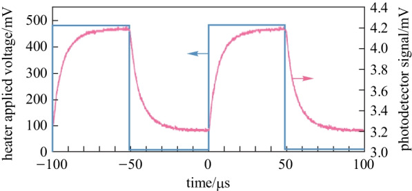
Temporal response of the TOPS with the 7-pass recycling structure. In all 1-pass, 3-pass, 5-pass, and 7-pass devices, the thermal time constant of rise time and fall time are (6.4 ± 0.2) and (6.6 ± 0.4) μs [61]
Therefore, the FOM of the 7-pass recycling-enhanced phase shifter is 11.1 mW/π·μs. It is smaller than for other TOPS, including those with the heater on a dense spiral waveguide (FOM = 33 mW/π·μs) and integrated doped-silicon heaters with adiabatic bends (FOM = 30.5 mW/π·μs). However, the insertion losses are about 1.2 dB (at the wavelength of 1570 nm), 2.2 dB (at 1594 nm), and 4.6 dB (at 1601 nm) for the 3-pass, 5-pass, and 7-pass structure, respectively (see Fig. 20).
Fig. 20.
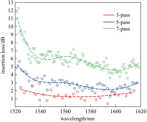
Insertion loss for three-, five-, and seven-pass devices as a function of wavelength, extracted from the MZI transmission spectra [61]
The disadvantage of this kind of structure is its large footprint and insertion loss. To solve this problem, we propose a new structure, as shown in Fig. 21a. An antisymmetric grating has been adopted to achieve mode conversation between TE0 mode and TE1 mode, which has a smaller size and lower insertion loss [61]. Unfortunately, the grating used to implement high-order mode conversation is complex. Therefore, the TOPS with only mode conversation of TE0 and TE1 based on antisymmetric grating has been fabricated on the CUMEC silicon platform. Compared with the TOPS of mode conversation via the asymmetric directional coupler, the footprint of this kind of TOPS is smaller. Moreover, Pπ is closer to one-third of that of the TOPS with one pass waveguide. Significantly, the mode conversion only happens between TE1 mode and TE0 mode, which can reduce the insertion loss effectively.
Fig. 21.
a Schematic of TOPS with multi-pass waveguide, the illustration figure is the schematic of the antisymmetric grating. b Curve of output light power versus the electrical driving power. c Fitting line of phase shift versus the electrical driving power. d Response curve of the TOPS is under 5.0 kHz
TOPS with the integrated diode
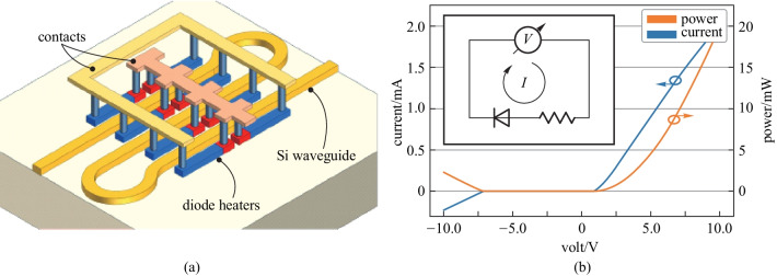
When the complexity of the large-scale photonic circuit increases, the circuit needs to be driven by means of hundreds or thousands of contact pads and voltage sources. The contact pads always occupy a large space in the photonic chip. Besides, a great number of wires are needed to connect the active devices to the pads. Therefore, the interfacing with electronics for controlling and read-out becomes a limiting factor for the scalability of the system. In recent years, Wim Bogaerts proposed a novel structure of TOPS with an integrated diode [62], as shown in Fig. 22. As mentioned earlier, doped silicon can be used as a resistor material to implement a TOPS on the SOI platform. Instead of either P-type or N-type dopants to increase the conductivity of the heater, the main body of the heater can use N-type dopants, and the region near one of the electrical contacts can be doped by P-type, creating a PN junction inside the heater. This approach converts the standard heater to a diode in series with a high resistivity strip. The total length of the heater is 50 μm, where 8 μm is used for the P-type doped region. The width of the heater is 1.2 μm. The heaters are placed closed to the target waveguide, keeping a gap of 0.75 μm between the heater and the waveguide. The gap was chosen to be close enough to increase the power consumption of the heater yet avoid leaking of the light from the waveguide to the heater. The heater and the waveguide have different widths to minimize coupling due to phase matching. The tuning efficiency of the TOPS is about 15–20 mW/π.
Fig. 22.
The schematic and experimental results of TOPS with the integrated diode [62]. a Phase shifter was implemented with eight diode heaters placed in parallel. b I–V curve showing the diode characteristic of the phase shifter. The inset figure is the equivalent electric circuit of the heater
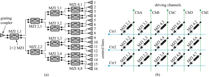
Furthermore, a diode-based TOPS in a matrix topology, grouping the heaters in sets of M columns and N rows, has been proposed and experimentally demonstrated, as shown in Fig. 23. In this arrangement, the anodes of the diode-heaters are connected in the same row together, while the cathodes are connected in the same column together. Here, the rows and columns of the matrix are defined as control lines and driving channels. It is possible to address one specific phase shifter in the matrix by setting the voltage level at its correspondent control line at a low level (GND) while setting the voltage of its correspondent driving channel at a high level (V+).
Fig. 23.
a 1 × 16 splitter tree circuit consisting of 15 tunable couplers, each of which is a balanced MZI with a TOPS in one arm. b Electrical connectivity of the 15 phase shifters. They contain a diode in series and are connected to three control lines and five driver channels [62]
Moreover, the matrix circuit can be divided into five identical sub-circuits along a single column, each containing one driving channel and three control lines, as shown in Fig. 24a. This requires a total of eight contact pads (and pulse width modulation (PWM) driving sources) to drive all 15 phase shifters needed to operate the circuit simultaneously. Figure 24b shows the time traces of a single driving channel in a circuit with N = 3 control lines.
Fig. 24.
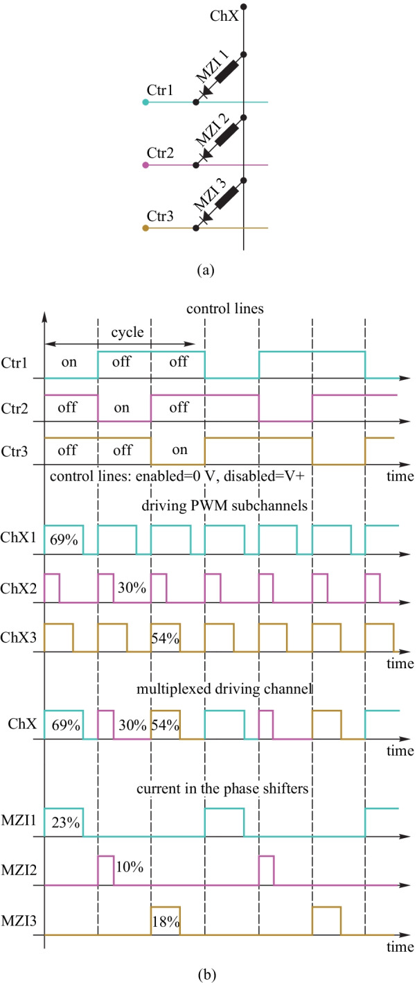
Time multiplexing the signals on the driving channel [62]. a A single driving channel ChX connecting three MZIs to control lines. b Control mechanism of the sub-circuit
In addition, time multiplexing has been adopted to improve the flexibility of this method. 1/N, where N is number of control lines, of the total cycle can be used by a TOPS at the same time. Therefore, the number of bond pads and power sources of a matrix arrangement that enables the driving of N × M phase shifters are (N + M) by using the PWM signal to implement multiplexed control. This technique is especially useful in silicon PICs with many TOPS devices but without enough space for electrical connections.
Discussion
As described above, there are many kinds of TOPS devices that use the SOI platform. Each kind of TOPS has advantages and disadvantages. To allow researchers to better choose the type of TOPS according to their demands, the performances of some typical TOPS are listed in Table 3. It is worth noting that the TOPS designed by the fabless organizations is not represented in Table 3.
Table 3.
Performance list of typical TOPS
| TOPS type | Silicon substrate undercut | Tuning efficiency/(mW·π–1) | Heating time/μs | Cooling time/μs | FOM/(mW·π–1·μs) | Footprint/(μm × μm) | Foundry | References |
|---|---|---|---|---|---|---|---|---|
| Doped silicon | N | 21.96 | 12.80 | 2.60 | 169.09 | 3.65 × 200 | CUMEC | [49] |
| Silicide | N | 21.75 | 12.90 | 4.00 | 183.79 | 3.65 × 200 | CUMEC | [45] |
| TiN | N | 19.12 | 5.90 | 8.97 | 142.15 | 2.0 × 200 | CUMEC | [45] |
| Folded waveguide | N | 2.75 | 21.1 | 8.1 | 40.15 | 59.0 × 278 | CUMEC | [45] |
| Multi-pass waveguide | N | 6.75 | 6.2 | 6.6 | 43.2 | 18.3 × 450 | CUMEC | [45] |
| Hybrid | N | 18.61 | 6.0 | 6.0 | 111.66 | 3.65 × 200 | CUMEC | [45] |
| Doped silicon | N | 20.4 | 21.3 | 66.0 | 890.46 | – | IMEC | [50] |
| Silicide | N | 22.5 | 19.1 | 75.8 | 1067.6 | – | IMEC | [46] |
| W | N | 23.4 | 38.2 | 45.1 | 974.61 | – | IMEC | [46] |
| Doped silicon | Y | 1.30 | 236 | 156 | 254.8 | – | IMEC | [46] |
| Silicide | Y | 1.49 | 188 | 218 | 302.47 | – | IMEC | [46] |
| W | Y | 1.42 | 198 | 227 | 301.75 | – | IMEC | [46] |
| TiN | N | 21.4 | 5.6 | NR | 119.84 | 7.5 × 320 | AMF | [15] |
| Doped silicon | N | 22.8 | 2.2 | NR | 50.16 | 4.1 × 320 | AMF | [15] |
| Silicide | Y | 20 | 2.8 | 2.2 | 50 | 3.5 × 200 | IBM | [16] |
| Doped silicon | Y | 24.77 ± 0.43 | NR | NR | NR | 3.0 × 61.6 | OpSIS | [51] |
| TiN | Y | 0.49 | 144.0 | 122.0 | 66.5 | 14 × 1000 | IME | [52] |
TiN: titanium nitride, W: tungsten, N: no, Y: yes, NR: not reported
As shown in Table 3, a heater in the TOPS is generally made of metal, doped silicon, or silicide on the SOI platform. For a TOPS with a basic structure, the tuning efficiency is about 20 mW/π. When the PIC consists of more than 1000 TOPS of this configuration, the power consumption would be more than 20 W. To reduce power consumption, further improvements should be made to improve the tuning efficiency of TOPS devices. Silicon substrate undercut is an effective way to improve the tuning efficiency of TOPS devices since the heat generated by the heater is mainly accumulated in the vicinity of the waveguide and does not leak to the environment. The tuning efficiency can be improved to about 1.50 mW/π, which is less than a tenth of that of a TOPS without silicon undercut. However, the thermal time constant of this structure is about 200 μs, which is unbeneficial for large-scale PICs. The requirement for TOPS devices for large-scale PICs, such as optical neural networks and optical phased arrays, are high tuning efficiency and fast switching time, i.e., small FOM. Moreover, a TOPS with a folded waveguide and multi-pass waveguide has been experimentally investigated to meet these needs. Unfortunately, the two kinds of TOPS would cause a higher insertion loss, which greatly limits the scale of an optical neural network or optical phased array. It is worth mentioning that the TOPS of a hybrid structure can improve the thermal time constant without sacrificing tuning efficiency and increasing insertion loss. This kind of TOPS has not been widely used in PIC since the improvement is not obvious. Besides, the thermal crosstalk effect can strongly affect the application of TOPS on PIC. To solve this problem, many approaches have been adopted, such as optimizing the chip layout, isolating thermal diffusion, developing temperature-insensitive devices, and packaging with a thermo-electric cooler (TEC).
Note that, high phase tuning efficiency is the requirement for all applications for TOPS devices. When the TOPS is used for adjusting the working point of the photonic device, such as the Mach–Zehnder modulator, fast switching time is not necessary. However, when the TOPS is used in reconfigurable silicon photonic circuits, such as optical neural networks, optical-path-routing switches, optical phased arrays, quantum processors, and programmable photonic circuits, high tuning efficiency and fast switching time are required at the same time. Furthermore, the scale of these circuits is closely related to the loss and footprint of TOPS. In summary, the TOPS with high phase tuning efficiency, fast switching time, low loss, and small footprint, is very promising for various applications on the SOI platform.
Conclusion
This work provides an overview of various TOPS devices on the SOI platform, together with a brief theoretical explanation and a review of the TOPS devices fabricated on different silicon foundry platforms. Compared with other foundries, the CUMEC silicon platform can provide both design and fabrication of all these TOPS devices at the same time. Low loss, small thermal time constant, higher phase tuning efficiency, and addressable TOPS devices are requirements for achieving further development.
Acknowledgements
This work was supported by Chuan-Yu Cooperation Project (No. Cstc2020jscx-cy1hX0006), Chongqing Science and Technology Commission of China (Grant No. cstc2020jscx-msxm0099 and cstc2020jscx-msxm0100), and Chongqing Natural Science Foundation of China (No. cstc2020jcyj-msxm3725).
Biographies
Shengping Liu
received his B.E. and Ph.D. degrees from Nanjing University, China, in 2014 and 2019, respectively. Currently, he is a full worker in Chongqing United Microelectronics Center (CUMEC). His research interests include thermo-optic phase shifter and optical neural networks.
Junbo Feng
received his B.E. and Ph.D. degrees from Huazhong University of Science and Technology, respectively. He studied in the electronic engineering department of Georgia Tech. during 2007.01–2008.06. After that, he continued his research at Peking University and Tsinghua University until 2011. Currently, he is the director of the silicon photonics center of Chongqing United Microelectronics Center (CUMEC). His research topics focus on silicon photonics and optical integration technologies.
Ye Tian
received his B.E. and Ph.D. degrees from Tongji University and National Center for Nano Science and Technology (NCNST), respectively in 2008 and 2013. After that, he worked at Hunan City University as a lecturer (2013–2015) and associate professor (2016–2019). In 2015–2016, he received a postdoctoral fellowship from the Chinese Scholarship Council (CSC) and worked at the photonics research group, Ghent University. Currently, he is a project manager at Chongqing United Microelectronics Center (CUMEC), focusing on photonics artificial intelligence chips.
Heng Zhao
received his master’s degree from Wuhan University in 2012. Currently, he is a regular employee of Chongqing United Microelectronics Center (CUMEC). His work focuses on silicon photonics packaging and testing technology.
Li Jin
received his doctoral degrees from Zhejiang University, China, in 2015. Currently, he is a full worker in Chongqing United Microelectronics Center (CUMEC). His research interests include optical phased array and external cavity laser.
Boling Ouyang
received a Ph.D. degree from the Delft University of Technology, Delft, The Netherlands, and published his thesis entitled “Integrated photonics interrogator and sensors for ultrasound detection.” After obtaining the Ph.D. degree, he joined Chongqing United Microelectronics Center (CUMEC), Chongqing, China as a research engineer and is working toward building programmable photonic integrated circuits.
Jiguang Zhu
received his Bachelor’s and Master’s degrees from Tsinghua University in 2000, and Zhejiang University in 2014 respectively. Zhu has 21 years of experience in semiconductor processing research and development. He is currently a full worker in Chongqing United Microelectronics Center (CUMEC) and is responsible for process development.
Jin Guo
received his Doctoral degree from Leuven University, Belgium, in 2008. Dr. Guo worked in IMEC from 2008 to 2011. Currently, he is the vice president of Chongqing United Microelectronics Center (CUMEC). His research interests include silicon photonics and optical integrated chips.
Author contributions
All authors have read and approved the final manuscript.
Declarations
Competing interests
The authors declare that they have no competing interests.
References
- 1.Su Y, Zhang Y, Qiu C, Guo X, Sun L. Silicon photonic platform for passive waveguide devices: materials, fabrication, and applications. Adv. Mater. Technol. 2020;5(8):1901153. doi: 10.1002/admt.201901153. [DOI] [Google Scholar]
- 2.Rahim, A., Spuesens, T., Baets, R., Bogaerts, W.: Open-access silicon photonics: current status and emerging initiatives. In: Proceedings of the IEEE, pp. 2313–2330. (2018)
- 3.Rahim A, Goyvaerts J, Szelag B, Fedeli J-M, Absil P, Aalto T, Harjanne M, Littlejohns C, Reed G, Winzer G, Lischke S, Zimmermann L, Knoll D, Geuzebroek D, Leinse A, Geiselmann M, Zervas M, Jans H, Stassen A, Domínguez C, Muñoz P, Domenech D, Lena A, Lemme MC, Baets R. Open-access silicon photonics platforms in europe. IEEE J. Sel. Top. Quantum Electron. 2019;25(5):1–18. doi: 10.1109/JSTQE.2019.2915949. [DOI] [Google Scholar]
- 4.Shen Y, Harris NC, Skirlo S, Prabhu M, Baehr-Jones T, Hochberg M, Sun X, Zhao S, Larochelle H, Englund D, Soljačić M. Deep learning with coherent nanophotonic circuits. Nat. Photonics. 2017;11(7):441–446. doi: 10.1038/nphoton.2017.93. [DOI] [Google Scholar]
- 5.Bogaerts W, Rahim A. Programmable photonics: an opportunity for an accessible large-volume PIC ecosystem. IEEE J. Sel. Top. Quantum Electron. 2020 doi: 10.1109/JSTQE.2020.2982980. [DOI] [Google Scholar]
- 6.Baghdadi R, Gould M, Gupta S, Tymchenko M, Bunandar D, Ramey C, Harris NC. Dual slot-mode NOEM phase shifter. Opt. Express. 2021;29(12):19113–19119. doi: 10.1364/OE.423949. [DOI] [PubMed] [Google Scholar]
- 7.Kang G, Kim SH, You JB, Lee DS, Yoo H, Ha YG, Kim JH, Yoo DE, Lee DW, Youn CH, Yu K. Silicon-based optical phased array using electro-optic p-i-n phase shifters. IEEE Photonics Technol. Lett. 2019;31:1685–1688. doi: 10.1109/LPT.2019.2939550. [DOI] [Google Scholar]
- 8.Quack N, Sattari H, Takabayashi AY, Zhang Y, Verheyen P, Bogaerts W, Edinger P, Errando-Herranz C, Gylfason KB. MEMS-enabled silicon photonic integrated devices and circuits. IEEE J. Quantum Electron. 2020;56(1):1–10. doi: 10.1109/JQE.2019.2946841. [DOI] [Google Scholar]
- 9.Yamashita T, Kim S, Kato H, Qiu W, Semba K, Fujimaki A, Terai H. π phase shifter based on NbN-based ferromagnetic Josephson junction on a silicon substrate. Sci. Rep. 2020;10(1):13687. doi: 10.1038/s41598-020-70766-9. [DOI] [PMC free article] [PubMed] [Google Scholar]
- 10.Landry A, Son TV, Haché A. Optical modulation at the interface between silicon and a phase change material. Optik (Stuttgart) 2020;209(6):164585. doi: 10.1016/j.ijleo.2020.164585. [DOI] [Google Scholar]
- 11.Kieninger C, Füllner C, Zwickel H, Kutuvantavida Y, Kemal JN, Eschenbaum C, Elder DL, Dalton LR, Freude W, Randel S, Koos C. Silicon-organic hybrid (SOH) Mach–Zehnder modulators for 100 GBd PAM4 signaling with sub-1 dB phase-shifter loss. Opt. Express. 2020;28(17):24693–24707. doi: 10.1364/OE.390315. [DOI] [PubMed] [Google Scholar]
- 12.Xie Y, Shi Y, Liu L, Wang J, Priti R, Zhang G, Liboiron-Ladouceur O, Dai D. Thermally-reconfigurable silicon photonic devices and circuits. IEEE J. Sel. Top. Quantum Electron. 2020;26(5):1–20. doi: 10.1109/JSTQE.2020.3002758. [DOI] [Google Scholar]
- 13.Qiao L, Tang W, Chu T. 32 × 32 silicon electro-optic switch with built-in monitors and balanced-status units. Sci. Rep. 2017;7(1):42306. doi: 10.1038/srep42306. [DOI] [PMC free article] [PubMed] [Google Scholar]
- 14.Edinger, P., Errando-Herranz, C., Gylfason, K.B.: Low-loss MEMS phase shifter for large scale reconfigurable silicon photonics. In: 2019 IEEE 32nd International Conference on Micro Electro Mechanical Systems (MEMS). IEEE (2019)
- 15.Jacques M, Samani A, El-Fiky E, Patel D, Xing Z, Plant DV. Optimization of thermo-optic phase-shifter design and mitigation of thermal crosstalk on the SOI platform. Opt. Express. 2019;27(8):10456–10471. doi: 10.1364/OE.27.010456. [DOI] [PubMed] [Google Scholar]
- 16.Campenhout JV, Green W, Assefa S, Vlasov YA. Integrated NiSi waveguide heaters for CMOS-compatible silicon thermo-optic devices. Opt. Lett. 2010;35(7):1013–1015. doi: 10.1364/OL.35.001013. [DOI] [PubMed] [Google Scholar]
- 17.Qiang X, Zhou X, Wang J, Wilkes CM, Loke T, O’Gara S, Kling L, Marshall GD, Santagati R, Ralph TC, Wang JB, O’Brien JL, Thompson MG, Matthews JCF. Large-scale silicon quantum photonics implementing arbitrary two-qubit processing. Nat. Photonics. 2018;12(9):534–539. doi: 10.1038/s41566-018-0236-y. [DOI] [Google Scholar]
- 18.Priti, R.B., Liboiron-Ladouceur, O.: A broadband rearrangeable nonblocking MZI-based thermo-optic O-band switch in the silicon-on-insulator. In: Advanced Photonics 2017 (IPR, NOMA, Sensors, Networks, SPPCom, PS). Optical Society of America, PM4D–2 (2017)
- 19.Horst F, Green WM, Assefa S, Shank SM, Vlasov YA, Offrein BJ. Cascaded Mach–Zehnder wavelength filters in silicon photonics for low loss and flat pass-band WDM (de-)multiplexing. Opt. Express. 2013;21(10):11652–11658. doi: 10.1364/OE.21.011652. [DOI] [PubMed] [Google Scholar]
- 20.Zhuang L, Zhu C, Xie Y, Burla M, Roeloffzen CGH, Hoekman M, Corcoran B, Lowery AJ. Nyquist-filtering (de) multiplexer using ring resonator assisted interferometer circuit. J. Lightwave Technol. 2016;34(8):1732–1738. doi: 10.1109/JLT.2015.2502251. [DOI] [Google Scholar]
- 21.Yu L, Yin Y, Shi Y, Dai D, He S. Thermally tunable silicon photonics microdisk resonator with graphene transparent nanoheaters. Optica. 2016;3(2):159–166. doi: 10.1364/OPTICA.3.000159. [DOI] [Google Scholar]
- 22.Guha B, Cardenas J, Lipson M. Athermal silicon microring resonators with titanium oxide cladding. Opt. Express. 2013;21(22):26557–26563. doi: 10.1364/OE.21.026557. [DOI] [PubMed] [Google Scholar]
- 23.Bahadori M, Gazman A, Janosik N, Rumley S, Zhu Z, Polster R, Cheng Q, Bergman K. Thermal rectification of integrated micro heaters for microring resonators in silicon photonics platform. J. Lightwave Technol. 2018;36(3):773–788. doi: 10.1109/JLT.2017.2781131. [DOI] [Google Scholar]
- 24.Pintus P, Hofbauer M, Manganelli CL, Fournier M, Gundavarapu S, Lemonnier O, Gambini F, Adelmini L, Meinhart C, Kopp C, Testa F, Zimmermann H, Oton CJ. PWM-driven thermally tunable silicon microring resonators: design, fabrication, and characterization. Laser Photonics Rev. 2019;13(9):1800275. doi: 10.1002/lpor.201800275. [DOI] [Google Scholar]
- 25.DeRose CT, Kekatpure RD, Trotter DC, Starbuck A, Wendt JR, Yaacobi A, Watts MR, Chettiar U, Engheta N, Davids PS. Electronically controlled optical beam-steering by an active phased array of metallic nanoantennas. Opt. Express. 2013;21(4):5198–5208. doi: 10.1364/OE.21.005198. [DOI] [PubMed] [Google Scholar]
- 26.Sun J, Timurdogan E, Yaacobi A, Zhan S, Hosseini ES, Cole DB, Watts MR. Large-scale silicon photonic circuits for optical phased arrays. IEEE J. Sel. Top. Quantum Electron. 2014;20(4):264–278. doi: 10.1109/JSTQE.2013.2293316. [DOI] [Google Scholar]
- 27.Huang C, Jha A, Lima TF, Tait AN, Shastri BJ, Prucnal PR. On-chip programmable nonlinear optical signal processor and its applications. IEEE J. Sel. Top. Quantum Electron. 2020;99:1–11. [Google Scholar]
- 28.Sugita A, Jinguji K, Takato N, Katoh K, Kawachi M. Bridge-suspended silica-waveguide thermo-optic phase shifter and its application to Mach–Zehnder type optical switch. IEICE Trans. (1976–1990) 1990;73(1):105–109. [Google Scholar]
- 29.Gu, J., Zhao, Z., Feng, C., Liu, M., Chen, R.T., Pan, D.Z.: Towards area-efficient optical neural networks: an FFT-based architecture. In: 2020 25th Asia and South Pacific Design Automation Conference (ASP-DAC), pp. 476–481. IEEE (2020)
- 30.Pour Fard MM, Williamson IAD, Edwards M, Liu K, Pai S, Bartlett B, Minkov M, Hughes TW, Fan S, Nguyen TA. Experimental realization of arbitrary activation functions for optical neural networks. Opt. Express. 2020;28(8):12138–12148. doi: 10.1364/OE.391473. [DOI] [PubMed] [Google Scholar]
- 31.Qin G, Zhu Q, Su Y. Fast wavelength seeking in a silicon dual-ring switch based on artificial neural networks. J. Lightwave Technol. 2020;38(18):5078–5085. doi: 10.1109/JLT.2020.3000531. [DOI] [Google Scholar]
- 32.Wang J, Bonneau D, Villa M, Silverstone JW, Santagati R, Miki S, Yamashita T, Fujiwara M, Sasaki M, Terai H, Tanner M, Natarajan CM, Hadfield RH, O’Brien JL, Thompson MG. Chip-to-chip quantum photonic interconnect by path-polarization interconversion. Optica. 2016;3(4):407–413. doi: 10.1364/OPTICA.3.000407. [DOI] [Google Scholar]
- 33.Wang J, Paesani S, Ding Y, Santagati R, Skrzypczyk P, Salavrakos A, Tura J, Augusiak R, Mančinska L, Bacco D, Bonneau D, Silverstone JW, Gong Q, Acín A, Rottwitt K, Oxenløwe LK, O’Brien JL, Laing A, Thompson MG. Multidimensional quantum entanglement with large-scale integrated optics. Science. 2018;360(6386):285–291. doi: 10.1126/science.aar7053. [DOI] [PubMed] [Google Scholar]
- 34.Silverstone JW, Bonneau D, Ohira K, Suzuki N, Yoshida H, Iizuka N, Ezaki M, Natarajan CM, Tanner MG, Hadfield RH, Zwiller V, Marshall GD, Rarity JG, O’Brien JL, Thompson MG. On-chip quantum interference between silicon photon-pair sources. Nat. Photonics. 2014;8(2):104–108. doi: 10.1038/nphoton.2013.339. [DOI] [Google Scholar]
- 35.Chung SW, Abediasl H, Hashemi H. A monolithically integrated large-scale optical phased array in silicon-on-insulator CMOS. IEEE J. Solid-State Circuits. 2018;53(1):275–296. doi: 10.1109/JSSC.2017.2757009. [DOI] [Google Scholar]
- 36.Van Acoleyen K, Bogaerts W, Jágerská J, Le Thomas N, Houdré R, Baets R. Off-chip beam steering with a one-dimensional optical phased array on silicon-on-insulator. Opt. Lett. 2009;34(9):1477–1479. doi: 10.1364/OL.34.001477. [DOI] [PubMed] [Google Scholar]
- 37.Chen S, Shi Y, He S, Dai D. Compact 8-channel thermally reconfigurable optical add/drop multiplexer on silicon. IEEE Photonics Technol. Lett. 2016;28(17):1874–1877. doi: 10.1109/LPT.2016.2574459. [DOI] [Google Scholar]
- 38.Bogaerts W, Pérez D, Capmany J, Miller DAB, Poon J, Englund D, Morichetti F, Melloni A. Programmable photonic circuits. Nature. 2020;586(7828):207–216. doi: 10.1038/s41586-020-2764-0. [DOI] [PubMed] [Google Scholar]
- 39.Pérez-López D, López A, DasMahapatra P, Capmany J. Multipurpose self-configuration of programmable photonic circuits. Nat. Commun. 2020;11(1):6359. doi: 10.1038/s41467-020-19608-w. [DOI] [PMC free article] [PubMed] [Google Scholar]
- 40.Liao S, Ding Y, Peucheret C, Yang T, Dong J, Zhang X. Integrated programmable photonic filter on the silicon-on-insulator platform. Opt. Express. 2014;22(26):31993–31998. doi: 10.1364/OE.22.031993. [DOI] [PubMed] [Google Scholar]
- 41.Xie Y, Zhuang L, Boller KJ, Lowery AJ. Lossless microwave photonic delay line using a ring resonator with an integrated semiconductor optical amplifier. J. Opt. 2017;19(6):065802. doi: 10.1088/2040-8986/aa6c0a. [DOI] [Google Scholar]
- 42.Hashizume Y, Katayose S, Tsuchizawa T, Watanabe T, Itoh M. Low-power silicon thermo-optic switch with folded waveguide arms and suspended ridge structures. Electron. Lett. 2012;48(19):1234–1235. doi: 10.1049/el.2012.1564. [DOI] [Google Scholar]
- 43.Densmore A, Janz S, Ma R, Schmid JH, Xu DX, Delâge A, Lapointe J, Vachon M, Cheben P. Compact and low power thermo-optic switch using folded silicon waveguides. Opt. Express. 2009;17(13):10457. doi: 10.1364/OE.17.010457. [DOI] [PubMed] [Google Scholar]
- 44.Smith, F., Wang, W., Wang, X., Li, Y., Cheng, X., Wu, H.: A design study of efficiency enhancement in silicon photonic thermo-optic phase shifters. In: 2019 IEEE Optical Interconnects Conference (OI). IEEE (2019)
- 45.Passaro V, Magno F, Tsarev A. Investigation of thermo-optic effect and multi-reflector tunable filter/multiplexer in SOI waveguides. Opt. Express. 2005;13(9):3429–3437. doi: 10.1364/OPEX.13.003429. [DOI] [PubMed] [Google Scholar]
- 46.De S, Das R, Varshney RK, Schneider T. Design and simulation of thermo-optic phase shifters with low thermal crosstalk for dense photonic integration. IEEE Access: Pract. Innov. Open Solut. 2020;8:141632–141640. doi: 10.1109/ACCESS.2020.3013116. [DOI] [Google Scholar]
- 47.Giuseppe C, Luigi S, Ivo R. Advance in thermo-optical switches: principles, materials, design, and device structure. Opt. Eng. (Redondo Beach, Calif.) 2011;50(7):071112. [Google Scholar]
- 48.Watts MR, Sun J, DeRose C, Trotter DC, Young RW, Nielson GN. Adiabatic thermo-optic Mach–Zehnder switch. Opt. Lett. 2013;38(5):733–735. doi: 10.1364/OL.38.000733. [DOI] [PubMed] [Google Scholar]
- 49.Liu, S., Tian, Y., Li, Y., Feng, G., Guo, J.: Comparison of thermos-optic phase-shifters implemented on CUMEC silicon photonics platform. In: Seventh Symposium on Novel Photoelectronic Detection Technology and Application. (2020)
- 50.Masood, A., Pantouvaki, M., Lepage, G., Verheyen, P., Van Campenhout, J., Absil, P., Van Thourhout, D., Bogaerts, W.: Comparison of heater architecture for thermal control of silicon photonics circuits. In: IEEE 10th International Conference on Group IV Photonics. IEEE (2013)
- 51.Harris NC, Ma Y, Mower J, Baehr-Jones T, Englund D, Hochberg M, Galland C. Efficient, compact and low loss thermo-optic phase shifter in silicon. Opt. Express. 2014;22(9):10487–10493. doi: 10.1364/OE.22.010487. [DOI] [PubMed] [Google Scholar]
- 52.Fang Q, Song JF, Liow TY, Cai H, Yu MB, Lo GQ, Kwong DL. Ultralow power silicon photonics thermo-optic switch with suspended phase arms. IEEE Photonics Technol. Lett. 2011;23(8):525–527. doi: 10.1109/LPT.2011.2114336. [DOI] [Google Scholar]
- 53.Lu, Z., Murray, K., Jayatilleka, H., Chrostowski, L.: Michelson interferometer thermo-optic switch on SOI with a 50-μW power consumption. In: 2016 IEEE Photonics Conference (IPC). IEEE (2016)
- 54.Sun P, Reano RM. Submilliwatt thermo-optic switches using free-standing silicon-on-insulator strip waveguides. Opt. Express. 2010;18(8):8406–8411. doi: 10.1364/OE.18.008406. [DOI] [PubMed] [Google Scholar]
- 55.Yu H, Ying D, Pantouvaki M, Van Campenhout J, Absil P, Hao Y, Yang J, Jiang X. Trade-off between optical modulation amplitude and modulation bandwidth of silicon micro-ring modulators. Opt. Express. 2014;22(12):15178–15189. doi: 10.1364/OE.22.015178. [DOI] [PubMed] [Google Scholar]
- 56.Song J, Fang Q, Tao SH, Liow TY, Yu MB, Lo GQ, Kwong DL. Fast and low power Michelson interferometer thermo-optical switch on SOI. Opt. Express. 2008;16(20):15304–15311. doi: 10.1364/OE.16.015304. [DOI] [PubMed] [Google Scholar]
- 57.Celo, D., Goodwill, D.J., Jiang, J., Dumais, P., Li, M., Bernier, E.: Thermo-optic silicon photonics with low power and extreme resilience to over-drive. In: 2016 IEEE Optical Interconnects Conference (OI). IEEE (2016)
- 58.Murray K, Lu Z, Jayatilleka H, Chrostowski L. Dense dissimilar waveguide routing for highly efficient thermo-optic switches on silicon. Opt. Express. 2015;23(15):19575–19585. doi: 10.1364/OE.23.019575. [DOI] [PubMed] [Google Scholar]
- 59.Chung S, Nakai M, Hashemi H. Low-power thermo-optic silicon modulator for large-scale photonic integrated systems. Opt. Express. 2019;27(9):13430–13459. doi: 10.1364/OE.27.013430. [DOI] [PubMed] [Google Scholar]
- 60.Qiu H, Liu Y, Luan C, Kong D, Guan X, Ding Y, Hu H. Energy-efficient thermo-optic silicon phase shifter with well-balanced overall performance. Opt. Lett. 2020;45(17):4806–4809. doi: 10.1364/OL.400230. [DOI] [PubMed] [Google Scholar]
- 61.Miller SA, Chang YC, Phare CT, Shin MC, Zadka M, Roberts SP, Stern B, Ji X, Mohanty A, Jimenez Gordillo OA, Dave UD, Lipson M. Large-scale optical phased array using a low-power multi-pass silicon platform. Optica. 2020;7(1):3–6. doi: 10.1364/OPTICA.7.000003. [DOI] [Google Scholar]
- 62.Alves AR, Declercq S, Khan MU, Wang M, Van Iseghem L, Bogaerts W. Column-row addressing of thermo-optic phase shifters for controlling large silicon photonic circuits. IEEE J. Sel. Top. Quantum Electron. 2020 doi: 10.1109/JSTQE.2020.2975669. [DOI] [Google Scholar]


