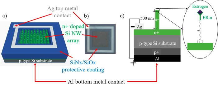
Figure 2.
(a) Schematic (not to scale) of the Si NW biosensor showing the key components of the p–n junction device, including the n+ doped Si NWs that are around 500 nm long, Ag top metal contact electrically connecting all the NWs, SiNx/SiOx dielectric stack that protects the metal contact from degrading during biofunctionalization steps, p-type Si substrate that is around 280 μm thick, and Al bottom contact. (B) Optical image of the top-view of the fabricated NW biosensor. The total sensor area is 11.5 mm by 11.5 mm, and after the SiNx/SiOx protective coating on the top metal contact, the exposed NW area is 6.2 mm by 6.2 mm. (C) Enlarged detail schematic (not to scale) of the cross-section of the biosensor showing the various doped regions, metal contacts, and ER-α functionalized NW surface. ER-α will become functionalized not only on the tip of the vSiNWs but also across the entire length of the vSiNWs. The schematic is simplified for clarity.

