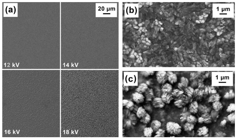
Figure 3.
SEM images of Cu-doped Sb2Se3 thin films deposited by LT-PED on Mo substrate: (a) a surface roughness comparison for samples deposited with different accelerating voltages; (b) a higher magnification of the sample deposited at 16 kV; and (c) a higher magnification of the sample surface deposited at 18 kV.

