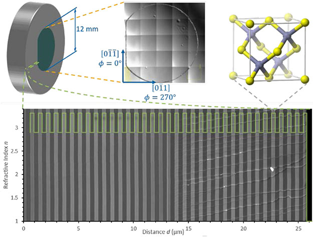
Fig. 1.
Details of the prototype mirror structure. Top left: Schematic of the 12 mm diameter crystalline coating bonded onto a Si substrate of 25.4 mm diameter with a concave 1 m radius of curvature. The flat is aligned with the [] crystal axis. Top middle: Stitched optical micrographs of the 12 mm diameter coating surface following the substrate transfer process. The values for ϕ refer to the relative polarization angle as defined later in Fig. 8. Top right: Zincblende structure of the crystalline coating (Ga in yellow, As in gray). Bottom: Cross-sectional SEM images of the layer stack consisting of 34.5 periods of alternating GaAs (light gray) and AlGaAs (dark gray) layers. The full coating was fabricated by stacking two intermediate structures grown with 17 periods capped with a 1/8th wave GaAs layer prior to substrate transfer. The bonding line is faintly visible in the middle of the centermost GaAs layer. Abrupt interfaces allow for precise measurements of individual layer thicknesses via edge detection (The green line indicates the refractive index profile). The terraced cracks in the cleaved coating (visible in the right half of the multilayer) result from a minute mismatch in crystal axis orientation from the stacking process, leading to an imperfect cleave of the top half of the mirror.

