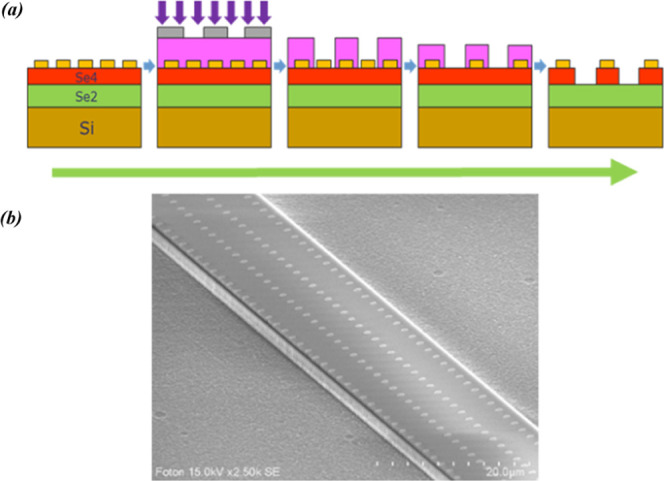
Figure 13.

Main steps of the technological procedure for the fabrication of SEIRA integrated selenide waveguides: (1) deposition of gold nanostructure; (2) photolithography; (3) development of the resin; (4) etching of the gold nanostructure; (5) fabrication of the rib waveguides by local etching of the chalcogenide guiding layer (a); SEM image of the SEIRA interface on selenide Se4/Se2 rib waveguides (b).
