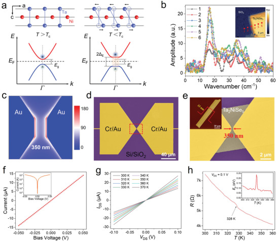
Figure 3.

Strong light–matter interaction and electrical properties of the Ta2NiSe5 photodetectors. a) Schematic diagram of the lattice distortion (upper panel) and the band structure (bottom panel) of Ta2NiSe5 crystals during the formation of EI state. b) Normalized THz near‐field signal spectra of the Ta2NiSe5 nanoflake at different positions. Inset is the THz near‐field microscopy (2nd order signal) mapping image. c) Electric field distribution in the bow‐tie antenna under 0.1 THz illumination. d,e) Full‐scale false color SEM image of the Ta2NiSe5‐based THz photodetector. Inset displays the AFM image of the Ta2NiSe5 nanoflake. f) I–V curve of the Ta2NiSe5 photodetector without gate voltage. Inset is the I–V curve in logarithmic scale. g) I–V curves of the Ta2NiSe5 device at different temperature. h) Resistance of the Ta2NiSe5 device as a function of temperature at V DS = 0.1 V. Inset shows the temperature dependence of the activation energy E ρ .
