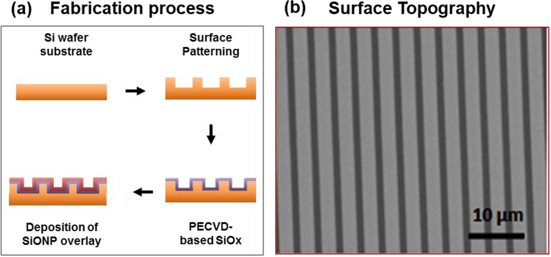
Figure 1.

Fabrication of SiONP overlays (a) A schematic diagram to illustrate the fabrication process for PECVD amorphous silicon oxynitrophosphide (SiONP) overlays with Si wafer substrate. (b) SEM micrograph shows the surface topography of a representative sample after photolithography, etching and PECVD deposition of SiONP (feature size 2 μm).
