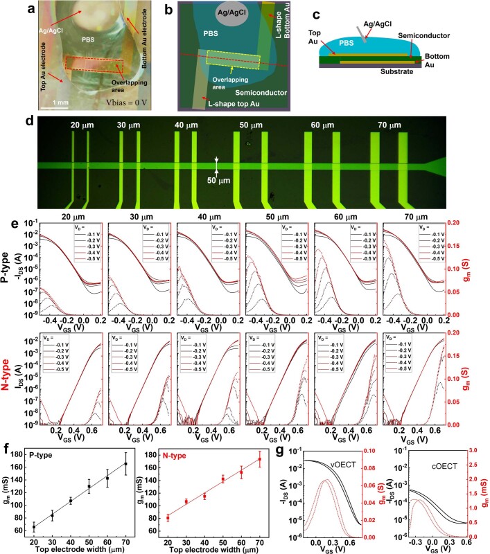
Extended Data Fig. 6. Vertical device structures for the direct observation of the electrochromic and performance characteristics of vOECTs with different top electrode widths.
a, Top view photograph and (b) corresponding p-type vOECT schematic indicating the large electrode overlapping area (~2 × 0.5 mm) used to monitor the electrochromic process associated to the redox chemistry of semiconducting layer. Here a L-shaped bottom Au electrode (100 nm thick) and an L-shaped top Au electrode (20 nm) are grounded and biased with −0.1 V, respectively. c, Cross section illustration of the vOECT from the indicated red dashed line in (b). d, Optical image of a p-type gDPP-g2T based vOECT array with different top electrode widths but identical bottom electrode. Note, these devices were fabricated by photolithography to accurately pattern the electrode dimensions and locate the semiconductor at the electrode cross points. e, Representative transfer characteristics of p-type and n-type (Homo-gDPP) vOECTs for the indicated top electrode width. f, Dependence of gm on top electrode width for the p- and n-type vOECTs, where VD = −0.5 V and 0.5 V, respectively. Data are from the average of 8 different devices. g, Transfer and gm characteristics of PEDOT:PSS based vOECTs (W = d = 30 µm) and cOECTs (W = 100 µm, L = 10 µm);, VD = −0.1 V.

