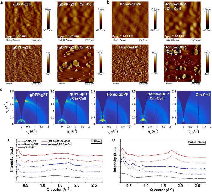
Extended Data Fig. 3. Semiconductor film morphologies and microstructures.
a, AFM height images and phase images of a pristine gDPP-g2T film and gDPP-g2T:Cin-Cell blend (9:2 in mass) film. b, AFM height images and phase images of a pristine Homo-gDPP film and a Homo-gDPP:Cin-Cell blend (9:2 in mass) film. c, 2D-GIWAXS images and corresponding (d) in-plane and (e) out-of-plane one-dimensional line-cuts for gDPP-g2T, gDPP-g2T: Cin-Cell, Homo-gDPP, Homo-gDPP: Cin-Cell, and Cin-Cell films. The gDPP-g2T in both pristine and blend films exhibits a preferential π-face-on orientation, yet with a considerable portion of crystallites being edge-on oriented. In all cases the lamellar and π-π periodicities are pinned at 20.2 Å and 3.6 Å, respectively. However, in both Homo-gDPP and Homo-gDPP:Cin-Cell the polymer orientation is preferentially edge-on and while the π-π distance is pinned at 3.6 Å, and the lamellar spacings vary slightly, from 20.2 Å to 19.6 Å, respectively.

