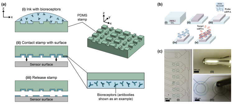
Figure 17.
(a) Illustration of the process to pattern a surface using µCP. (i) First, the elastomeric stamp is inked with a bioreceptor solution whereby bioreceptors adsorb to the stamp surface. Inking may be achieved using soak, spray-on, or robotic feature-feature ink transfer methods. Subsequently, the stamp can be rinsed and dried or used wet for stamping. (ii) The stamp is contacted with the sensor surface and gentle pressure is applied to transfer the bioreceptors from the stamp to the surface at the regions of contact. (iii) The stamp is released to reveal the bioreceptor-patterned surface. (b) Graphical representation of the functionalization of a SiP waveguide using tip-mold microcontact printing, showing the (i) waveguide cross-section of a reference microring, (ii) waveguide cross-section of a control microring, (iii,iv) application of ssDNA probes on the waveguide surface using a PDMS tip-mold µCP tool, and (v) hybridization of ssDNA targets to the immobilized ssDNA probes on the waveguide surface. (c) Images of (i) the SiP MRR sensor chip functionalized by Peserico et al. [202] via tip-mold µCP, (ii) the optical fiber tip with an unpatterned PDMS cladding used as the µCP tool, and (iii) example of bioreceptor application on MRR using µCP. Parts (b,c) are adapted with permission from Ref. [202]. Copyright 2017 The Institution of Engineering and Technology.

