
Figure 4.
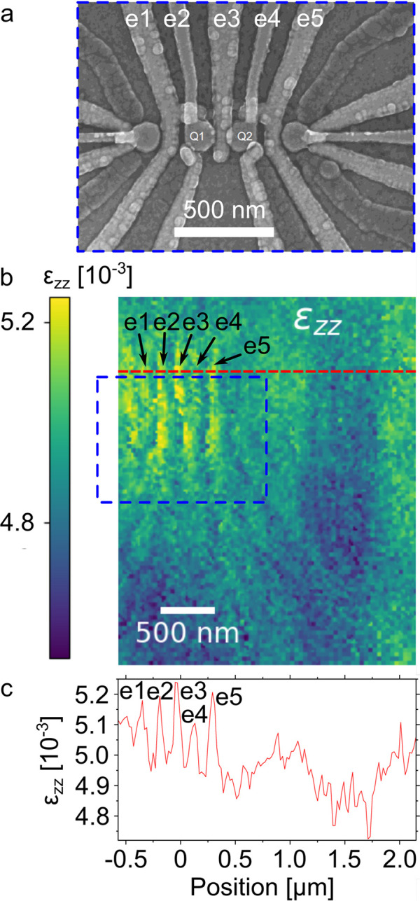
SEM image, εzz strain map, and strain line profile. (a) Top view SEM image of the qubit device. The QDs housing the two qubits are labeled with Q1, Q2 and the electrodes for qubit control with e1–e5. (b) Map of the εzz strain. The area in the blue box is the region shown in the SEM image. (c) Profile along the red line in (b).