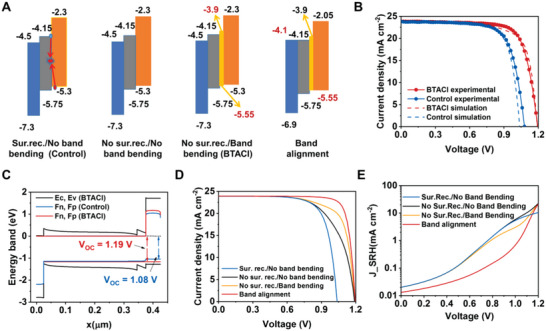
Figure 6.

The device physics modeling analysis. A) The structures and band diagrams of semiconductor layers in the simulation. B) J–V curves obtained from SCAPS simulation in comparison with the experimental results for the cases of the control and BTACl‐treated devices. C) Band diagrams and the quasi‐Fermi levels for the cases of the control and BTACl‐treated films. D) J–V curves obtained from SCAPS simulation for all cases. E) Shockley–Read–Hall (SRH) recombination current density revealed by SCAPS simulation.
