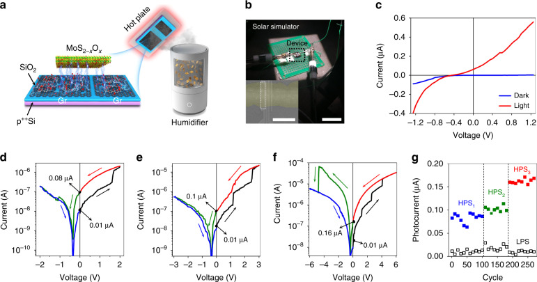
Fig. 1. The basic device with displaced and pinched hysteresis current-voltage characteristics.
a Schematic representation of the MoS2-xOx structure with CVD-grown graphene electrodes of different contact areas and the experimental process of LPE film deposition using the ultrasonic deposition setup. Spheres: carbon—black, oxygen—red, molybdenum—green, sulfur—yellow. b Optical image of the G/M/G device with solar light illumination. Scale bar, 2 cm. The inset shows an SEM image of another device, scale bar, 250 μm. the white rectangle indicates the area (256.2 × 62.5 μm2) of a G/M/G device. c Current-voltage characteristics of G/M/G devices at HPS in the dark (blue line) and in the light (red line). d–f Multilevel photoresponse switching characteristics at a discrete input bias voltage. g Endurance of photoresponse states (HPS1, HPS2, HPS3, LPS) over hundreds of switching cycles (reading at 0 V bias)

