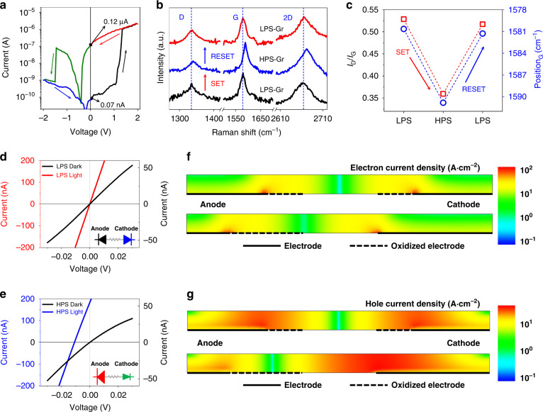
Fig. 2. Photoresponse switching mechanism.
a I-V characteristics of a G/M/G device with binary photoresponse switching when the voltage sweeps from 0 to 2 V, from 2 V to –2 V, and back to 0 V. b Raman curves showing the evolution of redox reactions on graphene electrodes when switching between HPS and LPS. c Correlation of changes in the ratio of the intensities of Raman scattering and shifts of the G mode of graphene electrodes and states of the non-volatile photoresponse. TCAD-simulated dark/photo current of the G/M/G device for LPS (d) and HPS (e). The insets of (d) and (e) demonstrate the qualitative device model for LPS and HPS, respectively. f The electron current density distribution of LPS (top) and HPS (bottom) under illumination, simulated with TCAD. g TCAD simulated the hole current density distribution of LPS (top) and HPS (bottom) under illumination, simulated with TCAD

