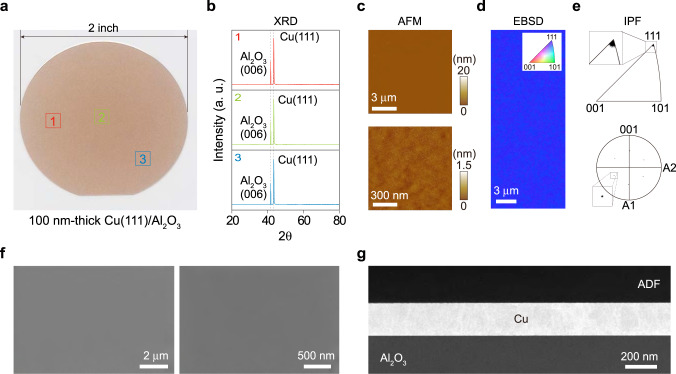
Fig. 2. Single-crystal Cu film (SCCF) grown by atomic sputtering epitaxy (ASE).
a Photograph of a 2-inch-diameter SCCF grown on Al2O3. b θ–2θ X-ray diffraction data taken at three different positions marked in a. c Surface morphologies at 20-nm (upper) and 1.5-nm (lower) vertical scales of atomic force microscopy (AFM) images with a root-mean-square surface roughness of 0.271 nm. d Electron backscatter diffraction (EBSD) map showing perfect alignment along the (111) plane. e Inverse pole figure (IPF) with a sole spot associated with the (111) plane (top) and [100] pole figure (PF) showing the six-fold symmetry of the {100} (bottom). The inset images in e are magnified images of the sole-spot areas. f Scanning electron microscopy images of the sample at different magnifications. g Low-magnification cross-sectional bright-field scanning transmission electron microscopy image of the SCCF sample.

