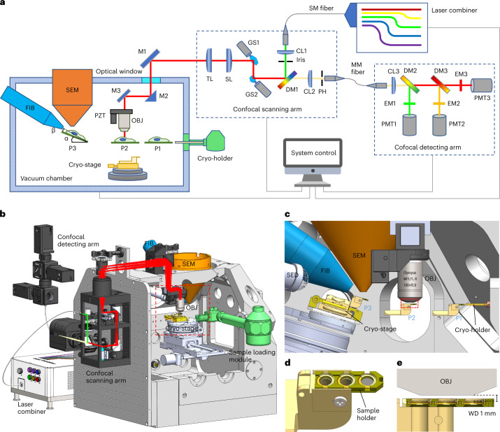
Fig. 1. Implementation of CLIEM.
a, Schematic diagram of the CLIEM system. α, Stage tilting angle during FIB milling; β, milling angle between the FIB and the sample plane; P1–P3, sample loading position (P1); LM imaging position (P2) and FIB–SEM position (P3). Abbreviations: objective (OBJ), piezo-stage (PZT), mirror (M), tube lens (TL), scanning lens (SL), galvo scanner (GS), collimating lens (CL), dichroic mirror (DM), pinhole (PH), single-mode (SM) fiber, multimode (MM) fiber and emission filter (EM). b, 3D rendering of the CLIEM system, showing the arrangement of the essential components and modules. c, The front view of the boxed area in b, illustrating the sample holder resting at three working positions (P1–P3). SED, secondary electron detector. d, 3D rendering of the sample holder containing three AutoGrid samples. e, The section view of the boxed area in c, displaying the 1 mm working distance (WD) of the confocal imaging module.

