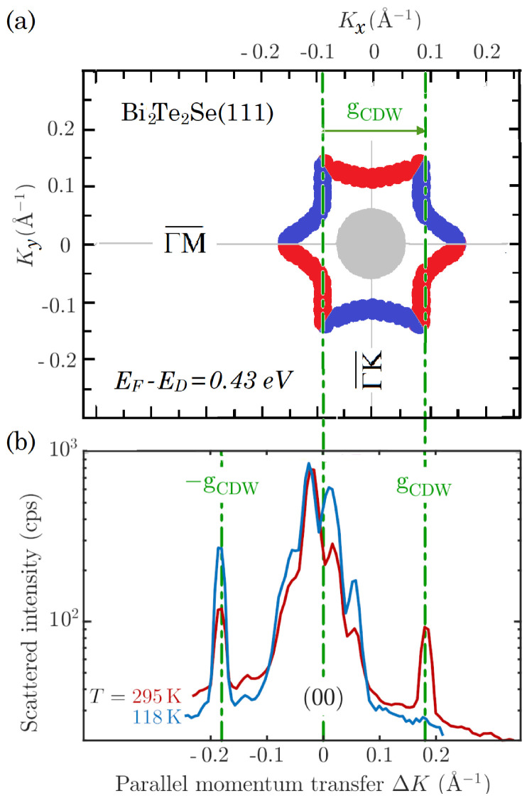
Figure 3.
Illustration of the spin-allowed nesting condition in (a), giving rise to the sharp CDW satellite peaks at around the -reflection in (b). HAS diffraction scans of BiTeSe(111) along the direction at room (295 K) and low (118 K) temperature in (b), show two sharp peaks at wavevectors , indicative of a surface CDW. While, at room temperature, the two diffraction peaks have about the same intensity, at K the peak intensity at is almost doubled at the expense of the peak at , which is vanishing. (a) The contours of the Dirac surface states at the Fermi level, derived from Nurmamat et al. surface band structure calculations [25] for a Fermi level eV above the Dirac point (see Figure 1c), form a hexastar (red and blue branches for states with spin-up and spin-down normal to the surface, respectively), with a clear nesting wavevector connecting parallel contours of equal spin. No such nesting occurs in the direction.

