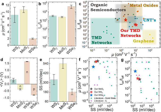
Figure 3.
Device performance compared to previous scientific literature. (a) Our transistor μ values for WS2, MoS2, and WSe2. (b) Our Ion/Ioff ratios for WS2, MoS2, and WSe2. (c) Our μ values and Ion/Ioff ratios (red stars) compared to those of other TMD networks (green triangles), organic semiconductors (black squares), metal oxides (orange pentagons), carbon nanotubes (blue circles), and graphene networks (yellow hexagons). (d) The device ⟨VT⟩ and (e) subthreshold slope for WS2, MoS2, and WSe2. (f) The μ and (g) Ion/Ioff ratio performance plotted as a function of the subthreshold slope for our electrochemical WS2, MoS2, and WSe2 transistors and compared in more detail to TMD networks for solid-state (green triangles) and ionically gated (purple pentagons) devices. Error is calculated by SDOM in this figure.

