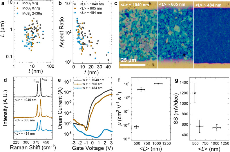
Figure 4.
Examination of the effect of ⟨L⟩ on MoS2 transistor performance. (a, b) Atomic force microscopy statistics of the MoS2 flakes. (c) Optical microscopy of the transistor channels with ⟨L⟩ from 484 to 1040 nm. (d) Raman spectroscopy of MoS2 to determine the defect density in the MoS2 flakes. (e) Transfer characteristics of the MoS2 flake networks as a function of ⟨L⟩. (f) Average μ and (g) average subthreshold slope of the MoS2 transistors as a function of ⟨L⟩. Error is calculated by the standard deviation of the mean (SDOM) in each case.

