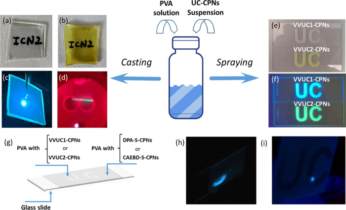
Figure 4.
Photographs of transparent (a) VVUC1-CPNs@PVA and (b) VVUC2-CPNs@PVA films under ambient light; photographs of (c) VVUC1-CPNs@PVA and (d) VVUC2-CPNs@PVA films showing UC emission under 532 and 650 nm CW laser irradiation, respectively; photographs of VVUC1-CPNs and VVUC2-CPNs spray-coated patterns under (e) ambient light and (f) UV irradiation (λexc = 365 nm); (g) scheme of the preparation of the material with a UC-based encrypted message; screenshots of the videos showing the UC emission of the spray-coated (h) VVUC1-CPNs- and (i) VVUC2-CPNs-based patterns while scanning with 532 nm (pulsed Nd:YAG) and 650 nm (CW) laser irradiation, respectively. UC emission only appears when the laser beam scans over the “UC” pattern. The beam spot of the 532 nm pulsed laser is large enough (1 cm diameter) to cover a surface area with and without VVUC1-CPNs, developing UC emission selectively in the area patterned with the UC nanoparticles (e.g., the bottom part of the “U” of the “UC” pattern as shown in Figure 4h).

