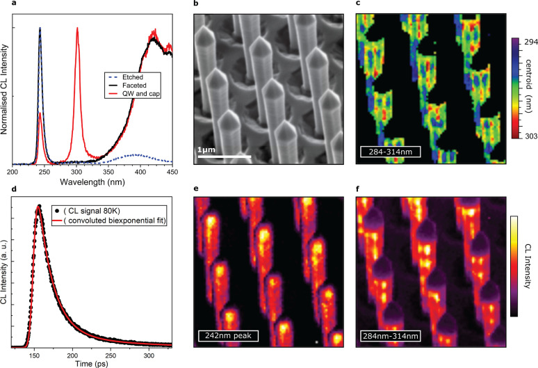
Figure 3.
Results from room-temperature, low-temperature, and time-resolved CL hyperspectral studies. (a) CL spectra from the three samples at room temperature: the etched cores, the etched cores following refaceting, and the etched cores following QW and cap growth. Each spectrum was taken by averaging a number of pixels from maps of each sample (taking care to avoid regions where the “substrate” was scanned directly) and was then normalized to a maximum. (b) Secondary electron (SE) image of the area mapped. (c) Map showing the shift in energy of the quantum well emission, with red shifts at the m-plane intersections (a plane). The noise-dominated substrate region has been masked in this map for clarity. (d) Fitted decay of the m-plane quantum well emission accounting for the instrument response function. (e) Map showing the uniform band edge emission peak intensity from the core. (f) CL intensity of the quantum well emission showing distinct high-intensity clusters at the a plane along with lower emission intensity from the rest of the m-plane sidewalls. Emission from the top semipolar facets is notably absent.

