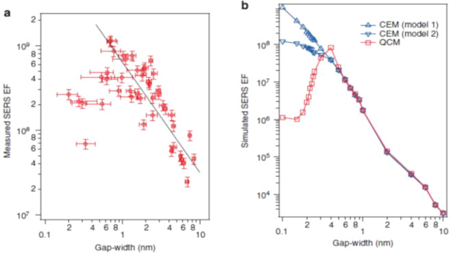
Figure 2.
Impact of the quantum mechanical electron tunnelling on the SERS EF. (a) Maximum SERS EFs for 45 dimers measured by wavelength-scanned SERS (red circles). The horizontal error bars represent the errors in the gap-width determination, which is retrieved following the procedures described in the Supporting Information of ref (70). The vertical error bars represent the errors in the SERS EF measurements, which are calculated from the uncertainties in the reference Raman measurements for neat thiophenol (Supporting Information of ref (70)). The gap-widths range from (2.0 ± 0.6) Å to (9.1 ± 0.4) nm. The maximum SERS EF measured is (1.2 ± 0.2) × 109 for dimer III with a gap-width of (6.7 ± 1.1) Å. Two regions that show opposite trends for the SERS EF as a function of the gap width are observed. For the gap width ranging from 6.7 Å to 9.1 nm, the measured SERS EF generally follows the phenomenological linear fit (in a log–log scale) as log(EF) = 8.8–1.3log(gap width). The SERS EF generally increases as the gap width decreases in this region. As the gap width further decreases from 6.7 to 2.0 Å, the SERS EF does not increase but instead decreases significantly. (b) Simulated SERS EFs using both the quantum-corrected model (QCM) and classical EM model (CEM) for gap widths ranging from 1 Å to 10 nm. Only the EM SERS EF is considered (see Methods), and the simulated EFs are one to 2 orders of magnitude smaller than the measured values, mainly due to SERS chemical enhancement. The CEM simulations of Model 1 assume monolayer coverage of the thiophenol molecules on the gold surfaces. The CEM simulations of Model 2 consider the hypothetical case for which the thiophenol molecules cannot access the narrowest regions of the gap. Reproduced with permission from ref (70). Copyright 2014 Nature Research.

