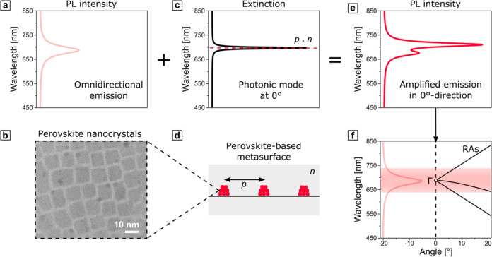
Figure 1.
(a) Omnidirectional emission of a thin film of CsPbI3 perovskite nanocrystals, shown in a transmission electron microscopy (TEM) micrograph (b). (c) Exemplary extinction spectrum from a grating, schematically shown in (d), under the normal incidence, featuring the photonic mode of the RA, defined by the product of the periodicity p, and refractive index of the environment n. (e) Modified emission of a perovskite-based metasurface with enhanced PL intensity in the normal direction. The spectra (a, c, e) were calculated analytically via Lorentzian functions and a coupled oscillator model.81 For more details, see Table S1 in the Supporting Information. (f) Exemplary dispersion diagram for 1D metasurface with p = 450 nm and n = 1.55. The positions of RAs, marked with solid black lines, and Γ point were calculated analytically with eq 1 and 2. The exemplary emission band of the CsPbI3 perovskites, spanning from 640 to 740 nm independently from the angle of incidence, is shown in light red.

