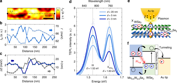
Fig. 2. Nanoscale heterogeneity of the interlayer coupling strength and TEPL of IX and .
a Hyperspectral TEPL image of the heterobilayer exhibiting inhomogeneous IX emission with 20 nm spatial resolution. b–c Spectroscopic and topographic line profiles for the dashed line L1 in (a). Nanoscale spatial heterogeneities in TEPL peak intensity IIX, linewidth Γ, peak energy shift ΔE, and topographic height ℎ are revealed far beyond the diffraction limit. d Evolving TEPL spectra of the heterobilayer as a function of the tip-sample distance d. The PL responses of IX (E = 1.52 eV) and WSe2 (E = 1.63 eV) are acquired with the tip located in the weak interlayer coupling region. e Illustration for the more efficient plasmon-IX (out-of-plane dipole) coupling compared to the plasmon-X (in-plane dipole) coupling when the Au tip closely approaches to the crystal. f Illustration for the type-II band alignment of a WSe2/Mo0.5 W0.5 Se2 heterobilayer and the work function of Au tip describing the charge transport mechanisms. This energy transfer mechanism explains our experimental results of increased (decreased) TEPL intensity of interlayer (intralayer) excitons when the tip approaches to the heterobilayer

