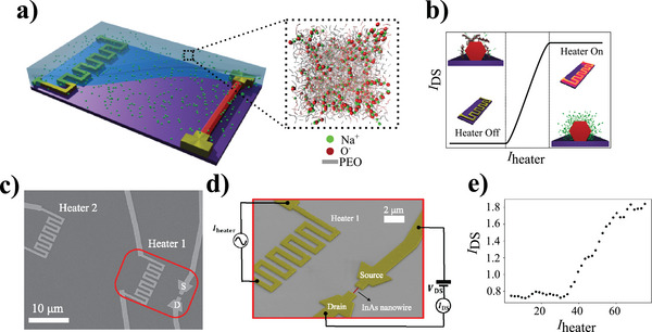
Figure 1.

Heat driven iontronic nanotransistor architecture and operation. a) Device pictorial view. A metallic serpentine acting as heater and an electrically contacted InAs nanowire are embedded into a polyelectrolyte. Inset: simulated molecular distribution of the polyelectrolyte at thermodynamic equilibrium. b) Current amplitude, I DS, in the nanowire versus heater current amplitude, I heater:expected behavior. Large I heater generates a temperature gradient driving net accumulation of Na+ ions at the polyelectrolyte/nanowire interface, yielding field effect modulation of I DS. c) Scanning electron micro‐graph of a prototypical device. Two heaters are positioned 7 and 35 µm away from the nanowire. d) Tilted scanning electron micrograph zoomed on the nanowire. The circuital scheme of the experimental setup, in overlay, shows the AC current generator feeding the heater, the voltage source and ampere‐meter for the measurement of the nanowire current. e) Typical heat‐driven device operation (I heater frequency 72 Hz, waiting time 120 s). I heater is found to drive a modulation of I DS reproducing the main features of the curve reported in panel (b). Here the maximum temperature difference, , between heater and nanowire is 0.6 K, as result from finite element analysis (Section S3, Supporting Information).
