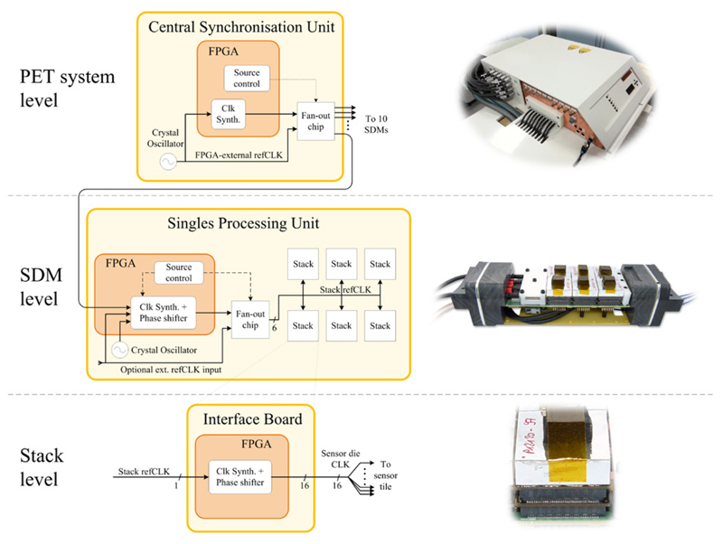
Figure 3.
Clocking infrastructure of the PET insert visualised for the reference clock (refCLK) and refCLK-derived clocks at PET system, SDM and stack levels. Arrows with dashed lines indicate clocking-related control signals, arrows with full lines indicate clock signal paths. At SDM level, the number of individual stack refCLK signal lines on the SPU is indicated by the number Six below the signal line close to the fan-out chip. The frequency and phase of the clock signals can be modified in each FPGA via integrated clock synthesizer and phase shifter blocks.

