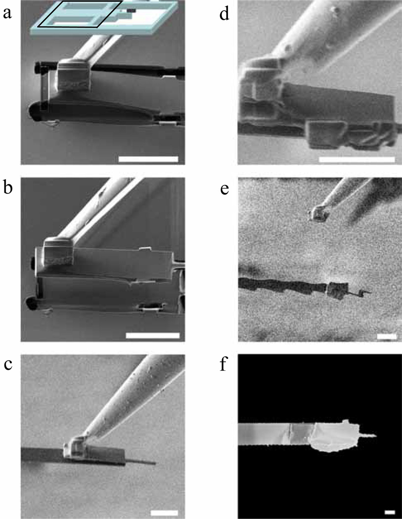
FIG. 3.
Ion-beam side-view (panels (a-e)) and SEM top-view (panel (f)) micrographs detail the magnet-tip liftout and cantilever-attachment procedure using a dual beam focussed-ion beam instrument. The inset in panel (a), which includes the chip device layer from Fig. 2(c), indicates the chip orientation and the box details the the visible region in the subsequent images. The process includes: (a) the probe tip is adhered to the magnet chip by FIB deposition of platinum; (b) the chip’s support tabs are milled and the chip is lifted out; (c) the chip is positioned over the cantilever’s leading edge and is brought into contact with the cantilever; (d) platinum deposition is used to adhere the chip to the cantilever; (e) the probe tip is milled and removed; and (f) the completed chip-on-cantilever. The serial attachment process takes 1.5 hours per fabricated chip-on-cantilever assembly, with an additional 0.5 hour for sample loading and unloading from the chamber. All scale bars are 5 µm.

