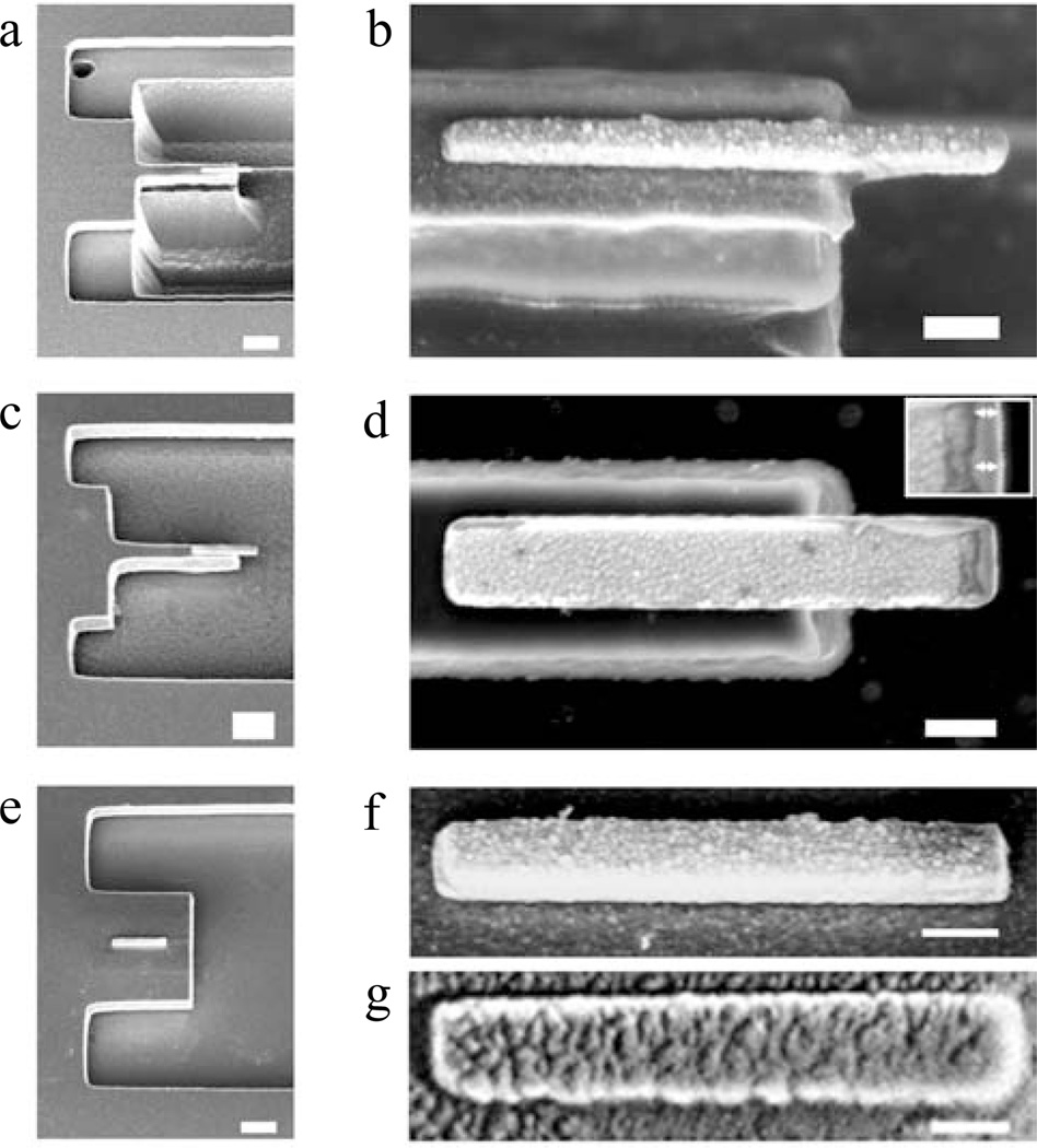
FIG. 4.
SEM images of the chip’s leading edge (left) and corresponding magnified images of the associated magnets (right) produced by three release protocols: a chip with an overhanging nanomagnet, released prior to magnet deposition by a BOE wet etch (a, b); a chip with an overhanging nanomagnet, released by HF vapor after magnet deposition (c, d); and a chip with a non-overhanging magnet, released prior magnet deposition with a BOE wet etch (e-g). It can be seen in the inset in panel (d) that releasing with HF vapor damaged the magnet’s leading edge; the arrows highlight the leading 20 nm of the magnet in which only the chromium adhesion layer is intact. The magnet in panel (g) is coated with approximately 6 nm of alumina prepared by atomic layer deposition. The magnets in panels (b) and (f) are undamaged and uncapped. The scale bar in (a,c,e) is 1 µm. The scale bar in (b,d,f,g) is 200 nm.

