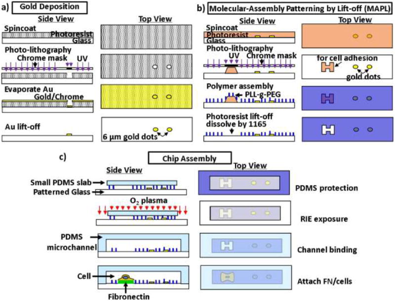
Figure 3. Schematic diagrams for microfabrication and chip assembly.

a) Pattern of gold dots on the glass substrate. b) Preparation of the glass substrate for cell patterning via MAPL. c) Assembly of the microfluidic channel with plasma bonding. See the materials table for the definitions of the abbreviations.
