Significance
Creating chiral nanostructures of semiconductors is fundamental for optoelectronic devices and metasurfaces with functionalities of chiral light manipulation and detection. However, this goal is largely hampered by current fabrication strategies which mostly lack the simplicity, controllability, versatility, and uniformity of the chiral nanostructures, especially for semiconductors. This work establishes a paradigm of creating chiral and complex platinum oxide with variable configurations simply by modulating the polarization of the laser beam. The polarized light induces synergistic effect of near-field–enhanced photochemical deposition and optical dipole interactions along the polarization, which is generally applicable to the growth of other semiconductors such as cadmium sulfide. It thus provides many opportunities for chiral metasurfaces, chiral luminescence and chiral optoelectronic devices.
Keywords: polarization, photochemistry, vector beam, chiroptics, CDS
Abstract
Chiral nanostructures based on semiconductors exhibit pronounced properties of chiral luminescence and optoelectronic responses, which are fundamental for chiroptoelectronic devices. However, the state-of-the-art techniques of generating semiconductors with chiral configurations are poorly developed, most of which are complicated or of low yield, rendering low compatibility to the platform of optoelectronic devices. Here we show polarization-directed oriented growth of platinum oxide/sulfide nanoparticles based on optical dipole interactions and near-field–enhanced photochemical deposition. By rotating the polarization during the irradiation or employing vector beam, both three dimensional and planar chiral nanostructures can be obtained, which is extendable to cadmium sulfide. These chiral superstructures exhibit broadband optical activity with a g-factor of ~0.2 and a luminescence g-factor of ~0.5 in the visible, making them promising candidate for chiroptoelectronic devices.
Chirality, a widely existed phenomenon on different scales of the universe, has attracted enormous interest for its fundamental understanding and practical applications (1–3). Chiral nanostructures based on semiconductors exhibit unique properties of chiral luminescence and optoelectronic response which are promising candidates for chiral information storage and chiral light detection (4, 5). Although a wealth of chiral materials exist in nature, mimicking and fabricating artificial chiral nanostructures for enhanced light-mater interaction appear challenging, especially for semiconductors (6). Most of previous approaches toward semiconductor chiral materials are based on wet chemistry (7–11), whose chirality is imparted by the chiral ligands or polymer templates. However, the dispersive nature of the chiral colloids makes them hard for chip integration with precise location and orientation, which is critical for the performance of chiral optoelectronic devices.
Light itself, carrying chiral information such as circular polarization (12–14) and vortices (15–17), can be transferred to materials with chiral configurations, which significantly reduces the fabrication difficulty of chiral nanostructures. However, this concept is largely restricted to polymers and metals. In some rare cases, circularly polarized light can generate chiral CdTe nanoribbons (18), but the chiral selectivity is small. Although the chiral selectivity can be improved with the assistance of plasmonic nanoparticles such as Au nanorods, the yield appears quite low as it is based on the plasmonic near field of single particle (12).
One facile way to build chiral nanostructures is to gradually rotate of the polarization during the growth, which establishes twisted chiral micropillars in three dimensions. However, this idea can hardly be achieved with previous techniques as it requires that the orientation of each layer is precisely controlled by the polarization. Although anisotropic growth directed by light polarization has been achieved in several plasmonic systems where enhanced local near field accelerates the growth/etching along the polarization (19–24), the plasmonic nanoparticles are indispensable for such oriented growth, which strongly limits their applicability to two-dimensional (2D) chiral nanostructures with low throughput (25). In this regard, photochemical growth intrinsically directed by the polarization is highly desired. Moreover, it can also be helpful to build in-plane chiral nanostructures by properly engineering the polarization directions via vector beam (26).
Here we show oriented growth of semiconductors, particularly platinum oxide/sulfide directed by the polarization of light without using any plasmonic nanoparticles. The platinum precursors ([PtCl4]−) are photolyzed and partially oxidized into platinum oxide nanoparticles with sizes of ~10 nm. These tiny nanoparticles show preferential growth along the laser polarization due to optical dipole forces and self-aligned near field, which eventually forms elliptical-shaped nanopillars. This polarization-directed oriented growth is also applicable for platinum sulfide and cadmium sulfide. By rotating the polarization direction during the irradiation, twisted chiral micropillars can be obtained which present optical activity in the visible with a g-factor up to 0.4. By using vector beam with engineered polarization, 2D spiral nanostructures can also be obtained, which present broadband chiroptic response in the visible. Moreover, the chiral structure of cadmium sulfide gives rise to a pseudochiral emission with a luminescence g-factor (glum) up to 0.5. This facile and versatile strategy unlocks a series of semiconductor chiral nanostructures, which can potentially serve as promising candidates for chiral metasurfaces and chiroptic devices.
Results
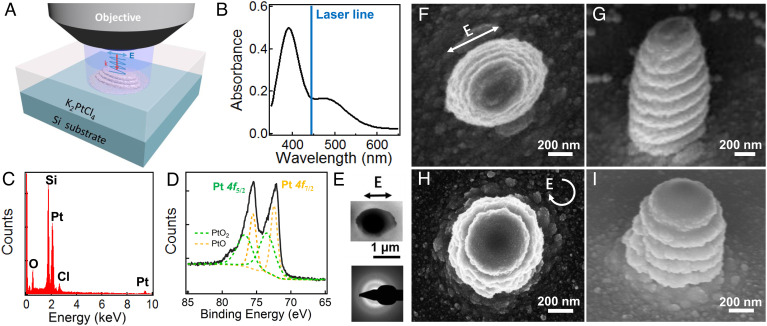
To optically grow platinum oxide nanopillars, plasma-cleaned Si substrate immersed in K2PtCl4 aqueous solution was irradiated by linearly polarized continuous wave (CW) laser (446 nm) under optical microscope (Fig. 1A). Since the K2PtCl4 solution shows strong absorbance in the near ultraviolet (Fig. 1B), it can be photochemically activated via the cleavage of the Pt–Cl bonds and photoaquation process (27), which eventually leads to the formation of platinum oxide nanoparticles. Energy-dispersive X-ray spectroscopy (EDS) suggests the photochemical products are mainly made of platinum and oxygen with residual chloride (Fig. 1C). X-ray photoelectron spectroscopy (XPS) shows the Pt ions are mainly in the higher valence state and spectral features (Fig. 1D) indicate that Pt exists in the form of Pt (II) and Pt (IV) as the Pt (II) are partially oxidized by the ionic radicals during the photolysis (SI Appendix, Supplementary Note 1) (28). Transmission electron microscope (TEM) confirms the elliptical shape of the Pt oxides, which are mostly amorphous as revealed by the diffusive electron diffraction (ED) pattern (Fig. 1E). Scanning electron microscope (SEM) characterization reveals the as-grown platinum oxide appears elliptical pillar-like nanostructure, whose orientation is along the polarization of the laser (Fig. 1 F and G). When the polarization direction changes, the orientation of the nanopillar changes accordingly (SI Appendix, Fig. S1). Irradiation by 532 and 641 nm CW laser can also lead to the oriented growth of platinum oxide nanoparticles into elliptical shape along the direction of laser polarization (SI Appendix, Fig. S2) but the growth efficiency is much lower with 641 nm laser due to the low absorbance of the K2PtCl4 over 600 nm (Fig. 1B). Changing the irradiation polarization to circular polarization generates circular nanopillars (Fig. 1 H and I), which indeed suggests the growth is polarization dependent.
Fig. 1.
Polarization-directed growth of platinum oxide nanopillars. (A) Schematic of the polarization-directed growth of platinum oxide. (B) Ultraviolet-visible absorbance of K2PtCl4 solution (10 mM). Blue line represents the irradiation beam wavelength. (C) EDS and (D) XPS spectra of the platinum oxide nanopillars. (E) TEM and ED images of a platinum oxide nanopillar. (F and G) SEM images of nanopillars irradiated by the linearly polarized CW laser (2 mW) for 30 s, (F) top view, (G) side view. The arrow in (F) indicates the polarization direction. (H and I) SEM images of nanopillars irradiated by the circularly polarized CW laser (2 mW) for 30 s, (H) top view, (I) side view. The arrow in (H) indicates the circular polarization.
The height of the nanopillars can be widely tuned by changing the concentration of K2PtCl4 solution, which can reach up to 1.5 μm within 10 s irradiation (SI Appendix, Fig. S3). Although increasing the concentration can also increase the aspect ratio of the nanopillars, it is more effective to increase the irradiation time to achieve large aspect ratio of the elliptical nanopillars (SI Appendix, Fig. S4). The growth seems to slow down after a minute’s irradiation with sizes around 1,000 nm for long axis, and ~600 nm for short axis and height (SI Appendix, Fig. S4G). This is likely because the as-grown nanopillars stick out the beam focal spot (~500 nm), which slows down the growth rate.
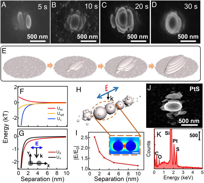
To carefully resolve their growth mechanism, we monitor the growth process at lower irradiation power, and take SEM characterization every 5 or 10 s of the irradiation (Fig. 2 A–D). Initially, only isolated ellipsoids are formed (Fig. 2A), which merges laterally in the first layer (Fig. 2B). The second and third layers form sequentially in the same fashion, which eventually evolve into nanopillars of elliptical shape (Fig. 2 C and D). Clearly, these nanopillars are assembled and grow from tiny platinum oxide nanoparticles, which are schematically depicted in Fig. 2E. The platinum oxide nanoparticles generated within the laser focal spot are charged with sizes around 20 nm as evidenced by the presence of spherical nanoparticles at initial stage of the growth (SI Appendix, Fig. S5). These nanoparticles are subject to electrostatic and van der Waals interactions as well as the optical dipole forces around the focal point. The former are isotropic, which equilibrate at certain separation, making the nanoparticles kinetically stable in solution. The latter is anisotropic which is related to the polarization of the laser. The optical dipole force can be numerically calculated by solving the Maxwell tensor (SI Appendix, Fig. S6) (29), while the electrostatic and van der Waals interaction can be analytically calculated based on DLVO theory (see SI Appendix, Supplementary Note 2 for the detailed calculation) (30). The calculated results of these three types of interactions (Fig. 2F), and their total energy potentials along X (polarization direction) and Y directions (Fig. 2G) suggest that it is kinetically more favorable for the platinum oxide nanoparticles to assemble and grow along the X direction, which leads to the anisotropic growth. Therefore, it is reasonable that the optical dipole forces along the polarization can induce the alignment of platinum oxide nanoparticles (Fig. 2H) and the self-enhanced electric near field between the platinum oxide nanoparticles further boosts the growth rate along the polarization (Fig. 2I). By the same mechanism, other semiconductor materials such as platinum sulfide (Fig. 2 J and K) and cadmium sulfide ellipsoids (SI Appendix, Fig. S7) can also be obtained (see SI Appendix, Supplementary Note 3 for the detailed photochemistry), suggesting the generality of this method.
Fig. 2.
Mechanism of polarization-directed oriented growth of platinum oxide nanopillars. (A–E) Evolution kinetics of platinum oxide nanopillars. SEM images of the platinum oxide nanoparticles at different irradiation time (A) 5 s, (B) 10 s, (C) 20 s, (D) 30 s. Irradiation power: 1 mW. (E) Schematic of the growth process. (F) Energy profile of the platinum oxide nanoparticles with optical dipole (Uopt), screening charge (Usc) and van der Waals (Uv) interactions and (G) the total energy along X and Y axis. The polarization is along X axis. Ux= Uopt + Usc + Uv and UY= Usc + Uv. (H) Mechanistic illustration on the polarization-induced charge dipole interaction. (I) Change of near-field enhancement with separation between the platinum oxide nanoparticles. Inset is the electric near field profile of two platinum oxide nanoparticles (dia. ~20 nm) with separation of 2 nm. (Scale bar is 10 nm.) (J) SEM images of PtS nanopillars formed by irradiating the mixture of K2PtCl4 and Na2S2O3 for 30 s (Irradiation power: 2 mW) and (K) corresponding EDS.
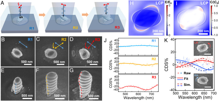
Since the growth orientation is directed by the polarization, we can rotate the polarization during the growth to obtain twisted micropillars (Fig. 3A). In this case, a half waveplate was applied to change the polarization direction by 45° for two times and the irradiation duration at each direction is ~5 s with total time of less than 20 s for each micropillar (see the experimental section for the details). We can generate arrays of such twisted micropillars via laser direct writing (SI Appendix, Fig. S8), and the typical SEM images of the irradiation products of three generations (R1 to R3) indeed exhibit strongly twisted morphology as the number of rotations increases (Fig. 3 B–G). Such twisted structures show different electric near-field profiles to the left and right circularly polarized (LCP/RCP) light, which appear mirror-symmetric (Fig. 3H and SI Appendix, Fig S9). The optical chirality (C) of this twisted structure can be calculated as (31)
| [1] |
Fig. 3.
Fabrication of twisted micropillars with rotating polarization and their optical activity. (A) Schematic of the fabrication of twisted micropillars with rotating polarization (R1: 0°, R2: 45°, R3: 90°) during the irradiation and (B–G) corresponding SEM images. (B–D) top views, (E–G) side views. Simulated near fields of (H) electric and (I) optical activity at the interface between two angled ellipsoids. Excitation source is LCP light at the dip (~650 nm) of CDS spectra. Averaged CDS spectra of (J) samples R1-R3 and (K) chiral enantiomers (R2). Insets are corresponding SEM images with scale bars of 500 nm. Dotted lines are the experimental raw data, solid lines are fitted CDS spectra and dash lines are calculated CDS spectra.
where and are the local magnetic field and conjugate of local electric field, respectively. Clearly, the twisted nanostructure presents superchiral field around the edges of the two ellipsoids at the interface, which indicates an optical chirality of ~−0.5 (Fig. 3I). This optical chirality directly correlates to the dissymmetric factor (g-factor), which can normally be characterized by the circular differential scattering (CDS) spectra (32, 33). For straight elliptical nanopillars, negligible CDS response is observed (Fig. 3J, R1). As the number of rotations increases, the CDS intensity increases proportionally with a g-factor up to 0.4 (Fig. 3J, R3).
Chiral enantiomers can also be obtained by rotating the polarization clockwise (right-handed, RH) and anticlockwise (left-handed, LH), which show inverted line shapes of CDS spectra (Fig. 3K). The simulated CDS spectra (dash lines) agree well with the experimental (solid lines), which further confirms the validity of the measurements.
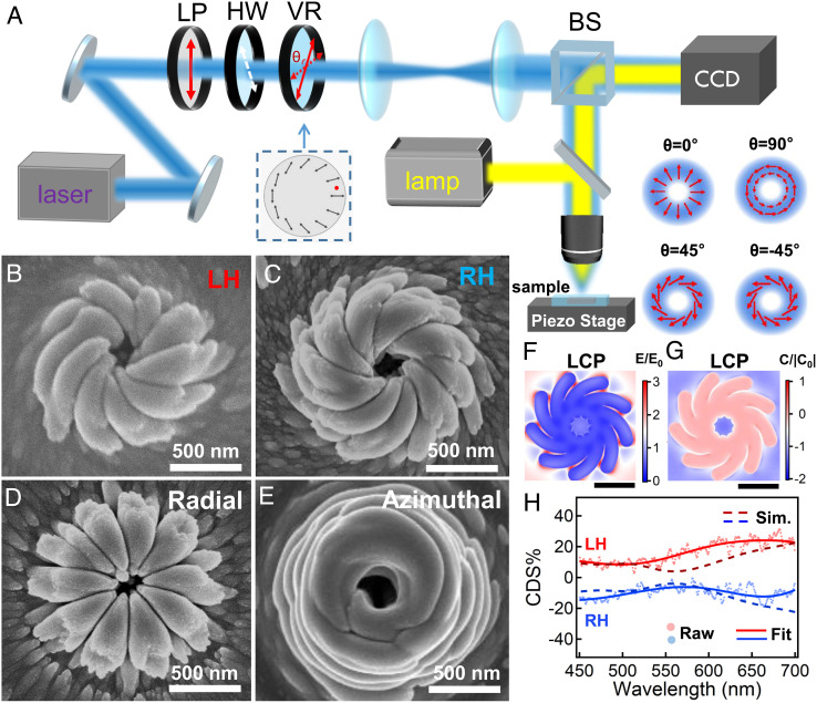
Another way to generate in-plane chiral structure is to use vector beam for the irradiation (Fig. 4A). The vector beam obtained by aligning the laser polarization to the fast axis of vortex retarder (VR) waveplate with certain angle (see experimental details) carries polarization with different arrangement (Insets at the Right Bottom of Fig. 4A). Since the growth is directed by the light polarization, platinum oxide nanoparticles can be arranged and grow into arrays of complex configurations as directed by the vector beams, which is also applicable to other semiconductors (SI Appendix, Fig. S10). SEM images reveal the as-grown platinum oxide nanostructure follows exactly the polarization profile in the vector beam (Fig. 4 B−E). Among them, the LH and RH enantiomers present spiral configuration, which show different electric field profiles in response to the LCP light (Fig. 4F and SI Appendix, Fig. S11). The optical chirality (C) again shows superchiral field with intensity up to −1.5 at center and −0.5 at the edges of the spiral nanostructures (Fig. 4G). The CDS spectra of the chiral enantiomers show broadband chiroptic response in the visible with a g-factor of ~0.2 (solid lines in Fig. 4H), which agrees well with the simulations (dash lines in Fig. 4H). This broadband g-factor is almost comparable to that of chiral plasmonic nanostructures (narrowband), which is an order of magnitude higher than most of the chiral semiconductors (SI Appendix, Table S1).
Fig. 4.
Fabrication of spiral nanostructures with vector beams and their optical activity. (A) Schematic of the fabrication setup for the generation of vector beam irradiation. LP: linear polarizer. HW: half-wave plate. VR: vortex retarder plate. BS: beam splitter. Insets at the Bottom Right corner show the polarization profile of vector beam generated with different alignment angle (θ). (B−E) SEM images of platinum oxide nanostructures generated by irradiating the K2PtCl4 precursor solution with different types of vector beams. (B) θ = −45° (C) θ = 45° (D) θ = 0° (E) θ = 90°. Simulated near field profile of (F) the electric and (G) the optical activity of spiral platinum oxide nanostructure. Scale bars are 2 μm. Excitation source is the LCP light at the peak (~510 nm) of CDS spectra. (H) CDS spectra of LH and RH enantiomers of platinum oxide. Doted lines are experimental raw data, solid lines are fitted data curves and dash lines are calculated CDS spectra.
The optical chirality is strongly affected by the structural chirality due to the chiral light-matter interactions. With increasing alignment angle from 0° to 90°, the structural chirality of spiral platinum oxide nanostructures first increases and then decreases, and their CDS response shows the same trend with the strongest intensity around 45° (SI Appendix, Fig. S12).
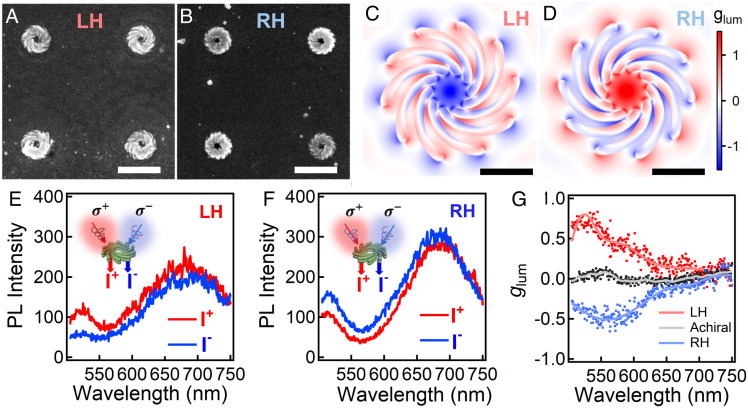
With such chiral light-matter interaction, chiral photoemission from chiral cadmium sulfide can also be observed but extremely weak with linear polarization excitation. With chiral excitation however, the enantiomers of cadmium sulfide (Fig. 5 A and B) can generate strong pseudochiral photoluminescence (PL), which can be estimated with the equation (34),
| [2] |
Fig. 5.
Chiral PL emission of chiral cadmium sulfide nanostructures. SEM images of (A) LH and (B) RH chiral cadmium sulfide nanostructures and (C and D) their simulated near field profile of the luminescence g-factor (glum). Scale bars in (A, B) and (C, D) are 2 μm and 500 nm, respectively. PL spectra of (E) LH and (F) RH cadmium sulfide nanostructures and (G) their glum spectra. I+ and I− denote the PL spectra detected with LCP (σ+) and RCP (σ−) excitation (446 nm), respectively. Insets are the schematics of the PL excitation and collection.
where and are local E-field at the wavelength of excitation and emission, respectively. The numerical results suggest a pseudochiral luminescence (SI Appendix, Fig. S13) with local glum up to 1.5 can potentially be produced with such chiral superstructures (Fig. 5 C and D). The chiral PL spectra from LH and RH structures of cadmium sulfide further verify this by presenting different PL intensities for LCP and RCP light excitation (Fig. 5 E and F), which give rise to an averaged glum of ~0.5 (Fig. 5G). For achiral nanostructures, the PL spectra reasonably present no difference from both excitations (SI Appendix, Fig. S14), which show negligible glum across the visible spectrum (grey line in Fig. 5G).
Discussion
In summary, we have demonstrated a facile and general strategy for the fabrication of oriented and chiral semiconductor nanostructures directed by the laser polarization. The precursors in principle should be photochemically active, which can be photolyzed into nanoparticles in aqueous solution. The polarization-induced optical dipole along with the enhanced near-field boost the oriented growth of ellipsoids. By gradually rotating the polarization during the irradiation, these ellipsoids stack into twisted micropillars. The polarization can also be engineered into vector beam, which directs the growth of nanoparticles into spiral superstructures. These chiral superstructures present broadband chiroptic response with a g-factor of ~0.2, which are promising candidates for the active control and manipulation of chiral light. This work offers a paradigm for the fabrication of a series of semiconductor chiral nanostructures, which opens a plethora of opportunities for chiral metasurfaces and chiral optoelectronic devices.
Materials and Methods
Precursor Solution Preparation.
Deionized (DI) water (from Millipore) was used for all the precursor solution preparation. For the growth of platinum oxide, potassium tetrachloroplatinate (Sigma-Aldrich) with typical concentration of 10 mM was prepared, which was then drop on (3-aminopropyl) triethoxysilane-functionalized glass or silicon substrate for laser irradiation. For the growth of sulfide, an aqueous solution of sodium thiosulfate (Na2S2O3, Macklin) was firstly prepared with concentration of 50 mM, which was then mixed with K2PtCl4 (10 mM) and CdCl2 (2 mM, aladdin) aqueous solution for the growth of PtS and CdS, respective under laser irradiation.
Irradiation Setup for Polarization Directed Growth.
A linearly polarized CW laser was free-space coupled into a customized upright microscope (BX53M, Olympus), which was then focused on silicon or glass substrates immersed in the precursor solutions mentioned above through a 100× dark-field objective (NA = 0.8, Olympus). The laser wavelength was 446 nm for all the irradiation unless stated otherwise. The irradiation power varied from 1 to 3 mW with duration of 1 to 60 s. The polarization of the laser beam can be modulated by rotating a half waveplate placed at the entrance of microscope (SI Appendix, Fig. S15). For the growth of 3D micropillars with twisted configurations, the half waveplate was programmed to rotate 22.5° with a motorized stage mount (KPRM1E, Thorlabs) after every irradiation (2 mW) of 3 to 7 s. To obtain planar complex nanostructures, the polarization of the CW laser was attenuated to be radially or azimuthally polarized by aligning the polarization along or vertical to the fast axis of a vortex retarder (VR1-442, LBTEK) plate, while for the spiral-like structures, the polarization and the fast axis of the VR plate was aligned in ±45° as shown in Fig. 4A. After the irradiation, all the samples were rinsed with DI water and blow-dried with nitrogen gun for further characterizations.
Characterizations.
XPS measurements were performed on a Thermo Fisher ESCALAB 250Xi instrument with a monochromatic Al K Alpha (1,486.68 eV) X-ray source and samples were measured under an ultrahigh vacuum (10−7 mbar). The X-ray HT was 15 kV, measured spot size was 200 μm. Charge neutralization was consistently provided by a flood gun with an internal magnetic lens. All the high-resolution spectra were obtained under CAE mode with pass energy of 25 eV, dwell time of 50 ms, and step size of 0.05 eV. SEM images and EDS of the oriented and chiral nanostructures were captured at the acceleration voltage of 5 kV and 20 kV, respectively. TEM image and electron diffraction pattern were obtained by JEM-2010FEF with acceleration voltage of 200 kV. Scattering spectra of the platinum oxide nanopillars were measured based on a home-built dark field microscope (BX53M, Olympus) with fiber-coupled spectrometer (QEPro, Ocean Optics). The CDS spectra of chiral nanostructures were collected with the same dark field setup with an additional set of linear polarizer and quarter waveplate placed in front of the halogen lamp. The polarization and fast axial direction of the quarter waveplate were aligned in ±45° to generate the incidence of left and right circular polarization (LCP/RCP). The scattering spectra of both LCP and RCP light on the chiral nanostructures ( and ) were collected with 50× DF objective (NA = 0.5, Olympus), and the CDS spectra are defined as,
| [3] |
The CDS spectra were fitted based on Gaussian peaks. Unless stated, all the CDS spectra were collected based on the individual chiral nanostructures, which were then averaged over five individuals to be more statistically representative.
For chiral PL spectra measurement, a 446-nm CW laser was used as the excitation source and a combination of half waveplate and quarter waveplate was applied to generate LCP and RCP excitations through a 100× objective (LMPLFLN100, Olympus). The luminescence g-factor is calculated based on the equation,
| [4] |
where and are the PL intensity excited with LCP and RCP light, respectively.
Simulations.
Finite-difference time domain method was applied to simulate the scattering spectra and near field distribution of the chiral nanostructures. Specifically, the total field scattering field was used as light source, perfectly matched layer was used as the boundary condition with a mesh size of 0.3 nm around the structures. The dielectric function of platinum oxide was calculated based on density function theory. The optical dipole forces and colloidal interactions were calculated based on Maxwell tensor equations and DLVO theory (see SI Appendix for the details).
Supplementary Material
Appendix 01 (PDF)
Acknowledgments
This research is supported by the National Natural Science Foundation of China (11974265) and the National Key Research and Development Program of China (2020YFA0211300). We thank the initial help of the project from Dr. Fangfang Deng. We also thank the support of the Centre for Nanoscience and Nanotechnology and Electron Microscope Centre at Wuhan University for SEM and TEM characterizations. The numerical calculations in this paper have been done on the supercomputing system in the Supercomputing Center of Wuhan University.
Author contributions
T.D. designed research; X.L., X.W., and Y.L. performed research; X.L., X.W., Y.L., and T.D. analyzed data; and T.D. wrote the paper.
Competing interests
A related patent (PCT/CN2021/073205) was filed on November 24, 2021.
Footnotes
This article is a PNAS Direct Submission.
Data, Materials, and Software Availability
All study data are included in the article and/or SI Appendix. The source data can be available from the authors or at figshare.com with the DOI: 10.6084/m9.figshare.20506809.
Supporting Information
References
- 1.Chen Y., et al. , Multidimensional nanoscopic chiroptics. Nat. Rev. Phys. 4, 113–124 (2022). [Google Scholar]
- 2.Lv J., et al. , Self-assembled inorganic chiral superstructures. Nat. Rev. Chem. 6, 125–145 (2022). [DOI] [PubMed] [Google Scholar]
- 3.Mun J., et al. , Electromagnetic chirality: From fundamentals to nontraditional chiroptical phenomena. Light Sci. Appl. 9, 139 (2020). [DOI] [PMC free article] [PubMed] [Google Scholar]
- 4.Li W., et al. , Circularly polarized light detection with hot electrons in chiral plasmonic metamaterials. Nat. Commun. 6, 8379 (2015). [DOI] [PMC free article] [PubMed] [Google Scholar]
- 5.Cai J., et al. , Polarization-sensitive optoionic membranes from chiral plasmonic nanoparticles. Nat. Nanotechnol. 17, 408–416 (2022). [DOI] [PubMed] [Google Scholar]
- 6.Ma W., et al. , Chiral inorganic nanostructures. Chem. Rev. 117, 8041–8093 (2017). [DOI] [PubMed] [Google Scholar]
- 7.Gao X., Han B., Yang X., Tang Z.. perspective of chiral colloidal semiconductor nanocrystals: Opportunity and challenge. J. Am. Chem. Soc. 141, 13700–13707 (2019). [DOI] [PubMed] [Google Scholar]
- 8.Qiao Y., et al. , Metal-driven hierarchical self-assembled one-dimensional nanohelices. Nano Lett. 9, 4500–4504 (2009). [DOI] [PubMed] [Google Scholar]
- 9.Sone E. D., Zubarev E. R., Stupp S. I., Semiconductor nanohelices templated by supramolecular ribbons. Angew. Chem. Int. Ed. 41, 1705–1709 (2002). [PubMed] [Google Scholar]
- 10.Feng W., et al. , Assembly of mesoscale helices with near-unity enantiomeric excess and light-matter interactions for chiral semiconductors. Sci. Adv. 3, e1601159 (2017). [DOI] [PMC free article] [PubMed] [Google Scholar]
- 11.Yan J., et al. , Self-assembly of chiral nanoparticles into semiconductor helices with tunable near-infrared optical activity. Chem. Mater. 32, 476–488 (2020). [Google Scholar]
- 12.Saito K., Tatsuma T., Chiral plasmonic nanostructures fabricated by circularly polarized light. Nano Lett. 18, 3209–3212 (2018). [DOI] [PubMed] [Google Scholar]
- 13.Liu T., et al. , Plasmonic nanocrystals for generation of hot electrons: Toward polarization-sensitive photochemistry. Nano Lett. 19, 1395–1407 (2019). [DOI] [PubMed] [Google Scholar]
- 14.Kim J.-Y., et al. , Assembly of gold nanoparticles into chiral superstructures driven by circularly polarized light. J. Am. Chem. Soc. 141, 11739–11744 (2019). [DOI] [PMC free article] [PubMed] [Google Scholar]
- 15.Toyoda K., Miyamoto K., Aoki N., Morita R., Omatsu T., Using optical vortex to control the chirality of twisted metal nanostructures. Nano Lett. 12, 3645–3649 (2012). [DOI] [PMC free article] [PubMed] [Google Scholar]
- 16.Ni J., et al. , Three-dimensional chiral microstructures fabricated by structured optical vortices in isotropic material. Light Sci. Appl. 6, e17011 (2017). [DOI] [PMC free article] [PubMed] [Google Scholar]
- 17.Liu L., et al. , Li Fast fabrication of silver helical metamaterial with single-exposure femtosecond laser photoreduction. Nanophotonics 8, 1087–1093 (2019). [Google Scholar]
- 18.Yeom J., et al. , Chiral templating of self-assembling nanostructures by circularly polarized light. Nat. Mater. 14, 66–72 (2015). [DOI] [PMC free article] [PubMed] [Google Scholar]
- 19.Violi I. L., Gargiulo J., von Bilderling C., Cortés E., Stefani F. D., Light-induced polarization-directed growth of optically printed gold nanoparticles. Nano Lett. 16, 6529–6533 (2016). [DOI] [PubMed] [Google Scholar]
- 20.Kim N. H., Meinhart C. D., M., Moskovits plasmon-mediated reduction of aqueous platinum ions: The competing roles of field enhancement and hot charge carriers. J. Phys. Chem. C 120, 6750–6755 (2016). [Google Scholar]
- 21.Chen C. J., Osgood R. M., Direct observation of the local-field-enhanced surface photochemical reactions. Phys. Rev. Lett. 50, 1705–1708 (1983). [Google Scholar]
- 22.Wang Y., et al. , Plasmon-directed polymerization: Regulating polymer growth with light. Nano Res. 11, 6384–6390 (2018). [Google Scholar]
- 23.Wang X., et al. , Polarization-controlled anisotropy in hybrid plasmonic nanoparticles. Nanophotonics 11, 1003–1009 (2022). [Google Scholar]
- 24.Ueno K., et al. , Nanoparticle plasmon-assisted two-photon polymerization induced by incoherent excitation source. J. Am. Chem. Soc. 130, 6928–6929 (2008). [DOI] [PubMed] [Google Scholar]
- 25.Besteiro L. V., et al. , Local growth mediated by plasmonic hot carriers: Chirality from achiral nanocrystals using circularly polarized light. Nano Lett. 21, 10315–10324 (2021). [DOI] [PMC free article] [PubMed] [Google Scholar]
- 26.Wang W.-Y., Cheng T.-Y., Bai Z.-X., Liu S., Lü J.-Q., Vector optical beam with controllable variation of polarization during propagation in free space: A review. Appl. Sci. 11, 10664 (2021). [Google Scholar]
- 27.Znakovskaya I. V., Sosedova Y. A., Glebov E. M., Grivin V. P., V. F., Plyusnin Intermediates formed by laser flash photolysis of [PtCl6]2− in aqueous solutions. Photochem. Photobiol. Sci. 4, 897–902 (2005). [DOI] [PubMed] [Google Scholar]
- 28.Broszkiewicz R. K., Grodkowski J., Pulse radiolysis studies on aqueous systems PtCl42− Cl− and PtCl42− Br−. Radiat. Phys. Chem. 8, 359–365 (1976). [Google Scholar]
- 29.Van Thourhout D., Roels J., Optomechanical device actuation through the optical gradient force. Nat. Photonics 4, 211–217 (2010). [Google Scholar]
- 30.Bishop K. J. M., Wilmer C. E., Soh S., Grzybowski B. A., Nanoscale forces and their uses in self-assembly. Small 5, 1600–1630 (2009). [DOI] [PubMed] [Google Scholar]
- 31.Tang Y., Cohen A. E., Optical chirality and its interaction with matter. Phys. Rev. Lett. 104, 163901 (2010). [DOI] [PubMed] [Google Scholar]
- 32.Karst J., et al. , Scatterometry on chemically synthesized single plasmonic nanoparticles. ACS Nano 13, 8659–8668 (2019). [DOI] [PubMed] [Google Scholar]
- 33.Smith K. W., et al. , Chiral and achiral nanodumbbell dimers: The effect of geometry on plasmonic properties. ACS Nano 10, 6180–6188 (2016). [DOI] [PubMed] [Google Scholar]
- 34.Gao H., Chen P.-G., Lo T. W., Jin W., Lei D., Selective excitation of polarization-steered chiral photoluminescence in single Plasmonic Nanohelicoids. Adv. Funct. Mater. 31, 2101502 (2021). [Google Scholar]
Associated Data
This section collects any data citations, data availability statements, or supplementary materials included in this article.
Supplementary Materials
Appendix 01 (PDF)
Data Availability Statement
All study data are included in the article and/or SI Appendix. The source data can be available from the authors or at figshare.com with the DOI: 10.6084/m9.figshare.20506809.


