Abstract
Functional materials are challenging to characterize because of the presence of small structures and inhomogeneous materials. If interference microscopy was initially developed for use for the optical profilometry of homogeneous, static surfaces, it has since been considerably improved in its capacity to measure a greater variety of samples and parameters. This review presents our own contributions to extending the usefulness of interference microscopy. For example, 4D microscopy allows real-time topographic measurement of moving or changing surfaces. High-resolution tomography can be used to characterize transparent layers; local spectroscopy allows the measurement of local optical properties; and glass microspheres improve the lateral resolution of measurements. Environmental chambers have been particularly useful in three specific applications. The first one controls the pressure, temperature, and humidity for measuring the mechanical properties of ultrathin polymer films; the second controls automatically the deposition of microdroplets for measuring the drying properties of polymers; and the third one employs an immersion system for studying changes in colloidal layers immersed in water in the presence of pollutants. The results of each system and technique demonstrate that interference microscopy can be used for more fully characterizing the small structures and inhomogeneous materials typically found in functional materials.
Introduction
Functionalized materials are very promising for use in new components, sensors, and technologies such as for example in protective layers, in self-repairing, or in chemical and biological detectors. To succeed, there is a need to be able to characterize the material properties at nano- and microscales and more and more often in carefully controlled environmental conditions.
Interference microscopy has developed into a widely used and useful technique for characterizing materials and providing rapid and quantitative measurements of microscopic surface topography.1 It is complementary to AFM and SEM, not having the same high resolutions but providing rapid measurements over large fields of view.2 Since interference microscopy uses an optical probe, at ICube (IPP photonics team), we have recognized for a long time that it is possible to extend the different possibilities in characterization with this technique, and the results of this work are summarized in this paper. Results are presented of measuring, for example, the 3D structure of changing surfaces in real time,3 visualizing and characterizing defects inside transparent layers,4 measuring the local optical properties of inhomogeneous materials using local spectroscopy,5 and observing and measuring details with higher lateral resolution using microspheres placed between the sample and the microscope objective.6,7
Some more recent applications have involved some challenging characterization conditions for measuring specific material parameters, notably requiring the development of environmental chambers placed under the interference microscope. We present some initial results of three interference microscope systems that have been combined with environmental chambers. The first one uses the control of the pressure, temperature, and humidity to measure the mechanical properties of ultrathin polymer films using the “nanobubble” technique.8 The second one uses the automatic control of the deposition of microdroplets to measure the drying properties of liquid polymers. The final one uses an immersion system for studying changes in colloidal layers immersed in water in the presence of heavy metals with an application in the study of pollution of the environment.9
With this review of the different techniques possible with interference microscopy, we show how we are moving toward multimodal microscopy, in which it is possible to make several types of measurements with the same interference microscope.
Basic Principles of Interference Microscopy
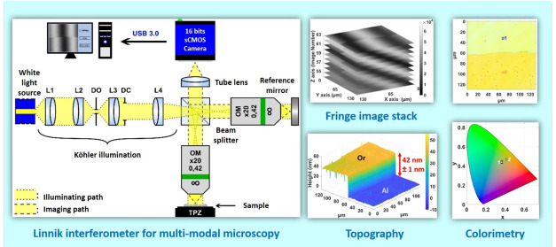
Interference microscopy is now commonly used in metrology for the measurement of surface roughness and microscopic 3D structures,1 and it is a complementary technique to SEM, AFM, and stylus profilometry.10 The main principle behind the technique is the use of white light interference fringes as a probe in an optical reflection microscope to determine the heights of the different points of a surface in order to build up its 3D structure. Figure 1(a) shows the breadboard Linnik microscope, using Köhler illumination with a white light LED (center wavelength of 660 nm, bandwidth of 380 nm) and a cube beam splitter to divide the illumination into two: one path for the sample and a second path for the reference mirror. In the Linnik configuration, two identical objectives are used, one in each path. The system uses two ×20 Mitutoyo long distance objectives (NA = 0.42), which have a long working distance and a large field of view. The reference and object beams are then recombined by the beamsplitter to form the interference image on the camera. A 16 bit Peltier-cooled camera with an sCMOS sensor (PCO Edge 4.2 USB3.0) having a spectral measurement range from 400 to 800 nm is used for low noise acquisitions. With a dynamic range of 91.5 dB, the noise level reduced to 0.3 electrons/pixel/s at 0 °C with a peak quantum efficiency of up to 82% at a wavelength of 590 nm, and this camera is particularly useful for measuring the large dynamic range of interference signals that can exist on certain samples. The system is controlled with a lab-developed LabVIEW program.
Figure 1.
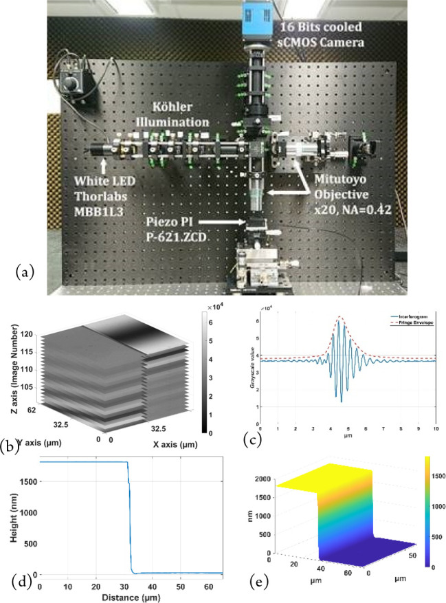
Linnik interference microscope system used for multimodal microscopy. (a) Experimental breadboard system with ×20 Mitutoyo long distance objectives with large field of view. Reproduced with permission from S. Marbach, C. Cordier, R. Claveau, T. Engel, P. Montgomery, M. Flury White Light Interference Microscopy System Design. Proceedings of SPIE Photonics Europe 2020 Digital Forum: Optics and Photonics for Advanced Dimensional Metrology; 2020; Vol. 11352.11 (b) XYZ stack of sampled fringe images on a calibration step etched in Si (VLSI SHS - 1.8 QC). (c) Intensity of interference fringes at one pixel. (d) 2D profile of step and (e) measured 3D structure of step after fringe processing using the FDA algorithm.
The sample is mounted on a piezo table to allow nanometer movement along the optical axis. A measurement is made by scanning the white light interference fringes over the whole depth of the sample at the step interval required for the fringe-processing algorithm used (typically λ/8 or 80 nm), giving a stack of images (Figure 1(b)). Using the FDA (frequency domain analysis) algorithm, based on Fourier transform processing,2 the topography of the surface can be determined at each point in the image, giving for example the step in Figure 1(c) and (d). While the Linnik configuration is flexible in its use and allows high numerical aperture objectives to be used, its difficulty in alignment reserves it mostly for use in research. For everyday measurements, the Mirau objective commonly found on commercial systems is more typically used.1 The technique has several advantages, the main one being a high nanometric axial sensitivity over a large dynamic range of tens of micrometers or more, limited only by the vertical scanning system. The measurements are also rapid, taking only several seconds to several minutes depending on the depth and the field size measured, which can vary from tens of micrometers to several micrometers.
Being an optical probe, it is nondestructive and can also be used for characterizing subsurface structures in transparent layers. The use of polychromatic light also means that it can be used to perform local spectroscopic measurements with the same system. With the lateral resolution being limited by diffraction, this limits the use of the technique to the measurement of structures 400 nm or more in size. These different aspects are dealt with in the rest of the paper.
Theory for Interference Microscopy
The intensity I of the interference fringe signal on the camera target at a pixel of the XYZ image stack (Figure 1(b)) is generally given as the following:
| 1 |
where φi is the known phase difference between the object and reference beams; ϕ(x,y) is the visibility of the fringe signal; and ϕ(x,y) is the unknown phase to be measured. Different algorithms exist for measuring this phase. In monochromatic illumination, the method of phase stepping microscopy (PSM) is generally used, by introducing known phase steps between the two paths and measuring the image intensity at each step. Different numbers of steps can be used, but the five-step technique is a good compromise between robustness and acquisition time:
| 2 |
The visibility γ(x,y) of the fringe signal can be determined from the following:
| 3 |
To measure the topography of the sample surface, the height at each point on the sample (x,y) is then determined from the following equation:
| 4 |
where θ and θ′ are, respectively, the angle of incidence and the angle of reflection with respect to the optical axis. This algorithm is generally used for measuring small surface roughness. For surface structures higher than λ/2, white light interferometry is used, in which polychromatic light produces an envelope of fringes (Figure 1(c)), the sum of the interference at the different wavelengths being:
| 5 |
where [λ1, λ2] is the spectral bandwidth of the light source and the term I0 takes into account the intensity and the spectral distribution of the light source, as well as the spectral response of the different optical components. The phase term ϕ, as well as being the difference in phase between the two paths of the interferometer, also takes into account the phase on reflection difference at the surfaces of the sample and reference mirror, which is also wavelength dependent. The peak of the envelope can be used to determine the position of the surface along the optical axis, different algorithms being used according to the application. The technique is classically used to make a single measurement at a time of static surface roughness or 3D structure, and the results in Figures 1(d) and (e) show the measurement of a calibration step etched in Si (VLSI SHS - 1.8 QC), with a quoted height of 1780.3 ± 11 nm.
Real-Time System, 4D Microscopy
While most surfaces in materials science are hard and static, more and more are not, especially among new functional materials and biological samples in which it may be necessary to measure crystal growth, liquids, gels or membranes.
While the characterization of periodic movement can be achieved by strobing, achieving real-time measurement of aperiodic movement while maintaining high image quality is more challenging. High bandwidths are first required for the data acquisition by the detector and then for the transfer of the data to the processor and the processing itself without the need for postprocessing.
In ref (3), we proposed a real-time 4D microscopy system using continuous fringe scanning over the depth of the sample to be measured, together with the use of a high-speed camera and wired logic for the processing (Figure 2(a)). This is achieved using a commercial CMOS camera (500–20,000 i/s) connected via CameraLink to a second-generation Virtex-II Pro FPGA (Xilinx) processing board. Two efficient algorithms for performing the signal processing were implemented in wired logic, the most compact based on the search for the maximum fringe intensity along the optical axis and the second based on the search for the maximum fringe visibility (eq 3). The latter, known as the five-step adaptive (FSA) algorithm,12 results in more robust measurements than the former. Data processing rates of 800 Mb/s–1.28 Gb/s are achieved with this system, resulting in real online measurements and recordable 3D results at a maximum rate of 22 topography maps per second for an image size of 256 × 320 pixels and 3 topography maps per second for an image size of 640 × 1024 pixels over a depth of 5 μm. The results in Figure 2(b) show two measurements made “on-the-fly” at a rate of 20 topography maps per second of a CMOS magnetic probe moving laterally at a speed of 200 μm/s (image size = 256 × 320 pixels, 600 × 750 μm). The camera image acquisition rate was 1320 frames per second, and a ×5 Michelson objective was used with the FSA algorithm.
Figure 2.
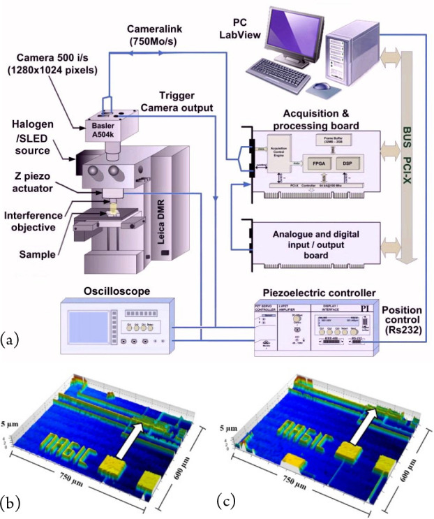
Real-time measurement system using a high-speed camera and FPGA processing: (a) schematic diagram of the acquisition, control, and processing system, (b), (c) two “on-the-fly” measurements made at 20 topography maps per second of a CMOS magnetic probe moving laterally (image size = 256 × 320 pixels, 600 × 750 μm). Reprinted with permission from Montgomery, P. C.; Anstotz, F.; Salzenstein, F.; Montaner, D. Real time and high quality online 4D FF-OCT using continuous fringe scanning with a high-speed camera and FPGA image processing. In Full-Field Optical Coherence Microscopy: technology and applications; Dubois, A., Ed.; Pan Stanford Publishing: Singapore, 2016; pp 393–428. Copyright 2016 Taylor and Francis Group.3
In such a system, the main speed limitations are related to the data transfer speed from the camera to the processing board, by the capacity and speed of the processing board itself, and of course to the Algorithm/Architecture Adequation (AAA) to implement the processing. Currently other high-speed communication buses would improve the performance related to the transfer rate between the camera and processing board (e.g., CoaXPress up to 25 Gb/s). The evolution of dedicated FPGA boards in principle would make it possible to envisage the real-time processing of data transmitted by the camera at these rates. However, image processing boards are mainly adapted to serial images by image processing, whereas in our algorithms we need to process a sliding window of several images over time (e.g., 5 images for the FSA algorithm). This requires significant temporary image storage buffers which are not often available on such boards.
Ideally a specific development of a camera associated with its processing circuit would allow the optimization of the suitable algorithm/architecture in each case.
Tomographic System for Acquiring Depth Images
To measure surface roughness with white light interferometry, a single fringe envelope is used, corresponding to the position of the surface (Figure 1(b)). If the fringes are scanned over the depth of a transparent layer, multiple signals are produced, each signal corresponding to a surface or a buried interface or structure (Figure 3(b)), often known as tomography or full field OCT.13 In these situations, the signal-to-noise ratio is generally much lower than for opaque/reflective structures, requiring optimization of the fringe acquisition method and image processing.
Figure 3.
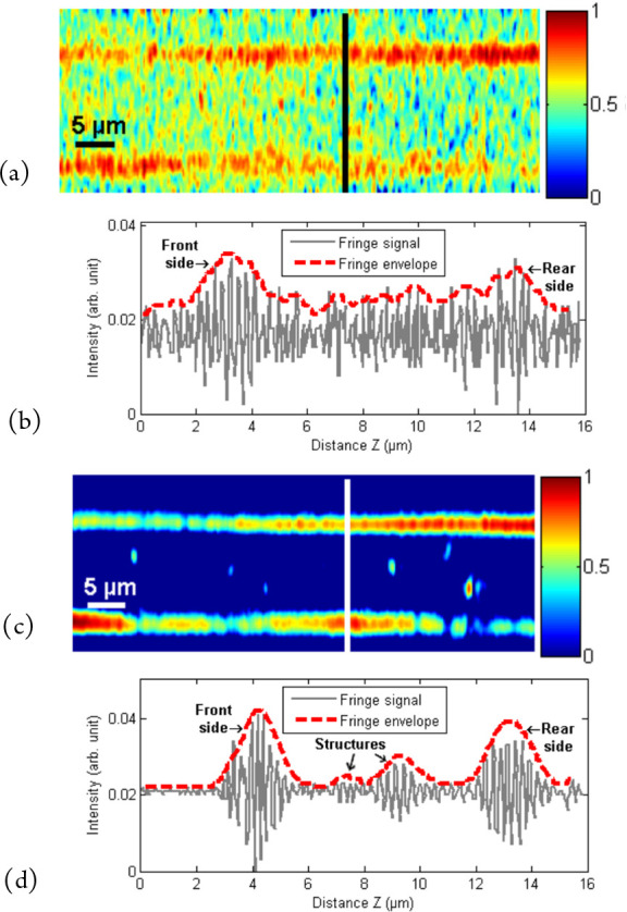
Tomography of a 6 μm thick “Mylar” polymer film using interference microscopy: (a) unprocessed cross-sectional profile (XZ image or “B” scan), (b) fringe signal (“A” scan) showing the presence of significant noise, (c) cross-sectional profile after averaging 100 images showing top and bottom surfaces and internal defects, and (d) fringe signal showing top and bottom surfaces and the presence of internal defects.
Several image acquisition and processing techniques are available, first to reduce the fixed pattern noise (FPN) using “dark” correction by subtracting an image taken without illumination of the camera target and then to correct the photoresponse nonuniformity (PRNU) or the variable gain between pixels using a “flat-field” acquisition.4 Then the dynamic range can be extended using the high dynamic range (HDR) method, taking several images with exposure bracketing to capture more of the different intensity levels as compared with a single shot.14,4 The important aspect to note with the latter technique is to provide a real increase in the dynamic range and not simply to improve the contrast of a fixed depth image as found in modern digital cameras. While the technique helps in measurements of a wider range of reflectance, on the downside, it is more sensitive to mechanical vibration, the measurement time increasing proportionally with the extra number of bracketing images taken.
One of the simplest and most efficient methods to reduce the noise is to carry out image averaging, the noise being reduced by a factor of √N, where N is the number of images used. The results in Figure 3 show the tomographic depth profile of a 6 μm thick Mylar polymer film. A single acquisition shows the presence of significant noise in the fringe signal or “A” scan (Figure 3(b)), which hides the details of the film in the XZ image or “B” scan (Figure 3(a)). The averaging of 100 images (Figure 3(c),(d)) clearly reduces the noise to reveal clearly not only the top and bottom surfaces but also defects within the thickness of the material (Figure 3(c)). The results were made on a modified Leitz–Linnik microscope with ×50 objectives and a Basler avA1000–100gc GigE CCD camera with a Giga Ethernet connection to the PC. This technique works well as long as the sample remains static and a short acquisition time is not important.15
Local Spectroscopy to Measure Local Optical Properties
If classical spectroscopy is the standard technique for obtaining the optical properties of materials, the large probe area of between several mm2 and 50 × 50 μm2 (spectroscopic ellipsometry) makes it difficult to probe local properties of inhomogeneous materials. Several techniques exist with local probes for measuring optical properties at a local scale, such as s-SNOM, hyperspectral imaging, and interference microscopy, which are described in this section.
The spectral analysis with interference microscopy is achieved by applying a Fourier transform to the interferometric signal (Figure 1(c)) taken over a small area, typically 0.325 × 0.325 μm2 in the present system. Its modulus gives the spectral response of the system multiplied by the sample and reference mirror reflectivities and is known as the noncalibrated spectral response (NCS):
| 6 |
To isolate the reflectivity of the sample, a calibration step is necessary, for example, by measuring the spectral response of a well-known sample such as a silicon wafer that has previously been measured with a classical spectrometer. This allows the optical properties of the system and reference mirror to be determined (Ssys(σ)·√[Rref(σ)]) or the spectral transfer function (STF). By keeping the same parameters of illumination intensity and optical arrangement as in the calibration step, the reflectivity of the sample can then be measured at each pixel in the image using the following formula:
| 7 |
For example, the results shown in Figure 4 show the local measurement of the reflectivity of a gold layer, with the uncalibrated spectra of gold and Si being shown in (a), the transfer function STF in (b), and the measured reflectivity of gold compared with theoretical values in (c).
Figure 4.
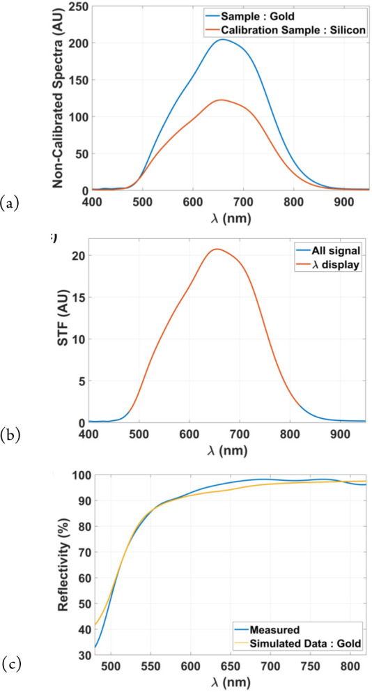
Performing local spectroscopy (0.325 × 0.325 μm2 measurement spot) on a gold layer using white light interference microscopy: (a) uncalibrated spectra of gold and Si, (b) spectral transfer function, and (c) measured reflectivity of gold compared with theoretical values.
By performing such a measurement at each pixel in the image, a spectral cube can be determined, providing spatially resolved spectral information, for example, on a step in a gold layer on an aluminum substrate (Figure 5(a)). This can then be used to extract different types of information, such as a spectral map at a specific wavelength (Figure 5(b)) or the spectral response of the different materials (Figure 5(c)).
Figure 5.
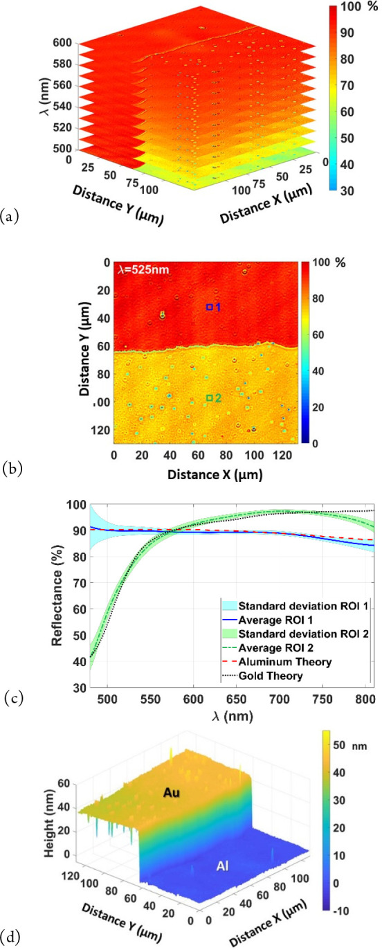
Multimodal microscopy characterization of the Au step on an Al substrate: (a) spectral cube to obtain spatially resolved (x,y) spectral information (λ), (b) reflectance map at λ = 525 nm from (a), (c) spectral response on small regions from (b) (10 × 10 pixels2, 3.25 × 3.25 μm2), and (d) 3D map of structure using the same data.
The same data can of course be used to measure the topography of the material (Figure 5(d)). In the case of conducting materials, the refractive indices are complex, leading to differences in the values of the phase on reflection and height measurement errors of up to a few tens of nm. While not significant on deep structures of several μm, in the case of nanometric steps as in this example, when measuring between Au and Al, it is 14.6 nm at a wavelength of 671 nm which has been added to the measured signal, giving the correct depth of 42 ± 0.5 nm in Figure 5(d), compared with 41 ± 3 nm by AFM. Identification of dissimilar materials and corrections in topography between them are now available on commercial instruments, for example, using model-based signal comparison.16
The principles of local spectroscopy can then be used in several different applications. For example, areas of different materials can be automatically identified, for example using Otsu’s algorithm to binarize the reflectivity map.5 The results can also be used in colorimetry to determine the colors of different materials. By windowing the fringe signal, this technique has also been adapted to performing local spectroscopy on interfaces and structures buried under transparent layers,17 for carrying out local measurements of refractive index and thickness of transparent layers,18 and for studying the properties of particles buried in transparent and diffusing layers.19
Improved Lateral Resolution Using Microspheres
While interferometry allows nanometric axial sensitivity for topographic measurement, the lateral resolution is several hundred nm, limited by diffraction. One way of improving the lateral resolution is to use a glass microsphere placed between the sample surface and microscope objective. This microsphere forms a magnified virtual image (Figure 6(a)) with a higher resolution than the microscope objective alone.20
Figure 6.
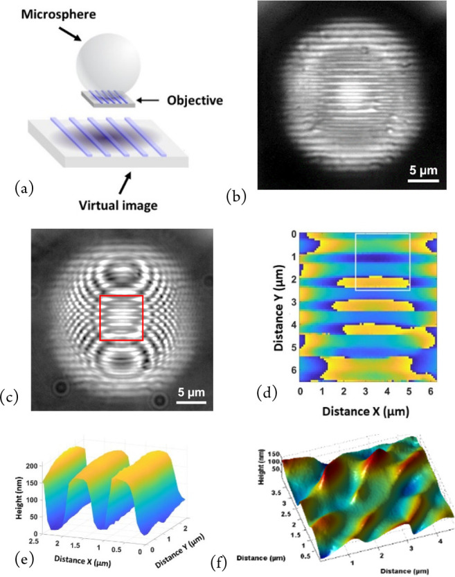
Microsphere-assisted microscopy using 130 μm diameter glass microspheres: (a) Schematic drawing of virtual image formation. Reprinted with permission from Perrin, S.; Li, H.; Leong-Hoï, A.; Lecler, S.; Montgomery, P. C. Illumination conditions in microsphere-assisted microscopy. J. Microsc. (Oxford, U. K.)2019, 274, 1, 69–75. Copyright 2019 Wiley.20 (b) Focused on a 1.2 μm period grating through a 130 μm diameter microsphere, not visible directly with the ×20 objective, (c) fringes superimposed on an image of grating through a microsphere, (d) PSM measurement with phase discontinuities (central part from (b)), (e) topography measurement after removal of curvature due to spherical aberration (from (d)), and (f) nanoripples on stainless steel measured with a 25 μm diameter microsphere. Reprinted with permission from Leong-Hoï, A.; Hairaye, C.; Perrin, S.; Lecler, S.; Pfeiffer, P.; Montgomery, P. High resolution microsphere-assisted in-terference microscopy for 3D characterization of nanomaterials. Phys. Status Solidi A2017, 215, 1700858. Copyright 2017 Wiley.6
For example, the 1.2 μm period grating in Figure 6(b) can be clearly resolved through the microsphere in this direct image but is not visible directly with the ×20 objective used. Adding fringes superimposed on the image of the grating (Figure 6(c)) shows that the interferometer is still sensitive to the phase of the light reflected from the surface structure through the microsphere. The use of PSM measurement on these fringes results in a phase measurement (with discontinuities), the central part of which can be usefully employed for the topography measurement (central part from (b)) in Figure 6(d), resulting in the 3D image in Figure 6(e).
The improvement in resolution using microsphere-assisted microscopy was determined by measuring the contrast of a series of contrast gratings (square profile Si/glass) with different periods from 0.2 to 5 μm in steps of 0.2 μm (Figure 7(a)). With the objective alone, the cutoff spatial frequency is better with the aperture diaphragm (AD) open, about 1.06 cycles/μm (0.94 μm) (red curve), being 0.86 cycles/μm (1.16 μm) for the closed AD (blue curve), in agreement with the theory for resolution of a microscope as a function of the spatial coherence of the illumination.
Figure 7.
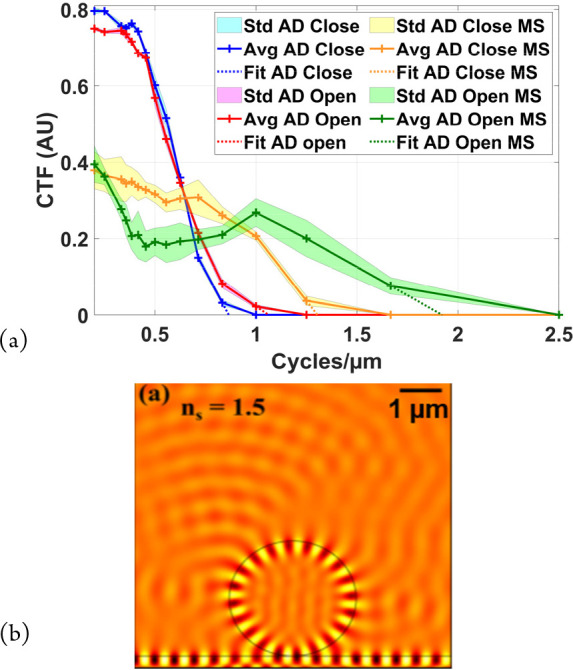
Study of nanometrology using microsphere-assisted Linnik interferometry: (a) contrast transfer function (CTF) of breadboard Linnik determined with the aperture diaphragm (AD) open/closed (red/blue) and then assisted with a 130 μm diameter glass microsphere with the AD open/closed (green/orange), (b) simulation showing the real part of the electric field distribution and the conversion of an evanescent wave into a propagating wave by a glass microsphere (ns = 1.5, λ0 = 600 nm, D = 3 μm). Reprinted with permission from Boudoukha, R.; Perrin, S.; Demagh, A.; Montgomery, P.; Eddine Demagh, N.; Lecler, S. Near- to Far-Field Coupling of Evanescent Waves by Glass Microspheres. Photonics2021, 8, 3, 73. Copyright 2021 MDPI.21
The cutoff frequency with the microsphere is also higher with the AD open, at 1.92 cycles/μm (0.52 nm) compared with the closed result, at 1.3 cycles/μm (0.77 nm). These results also show that there is a loss of contrast through the microsphere by about a factor of 2, probably due to imperfections inside the microsphere or the type of illumination used. The important point to note is the increase in lateral resolution from 0.94 to 0.52 μm with a 130 μm diameter microsphere. Other studies we have carried out show that the resolution increases with decreasing microsphere diameter but that the useful field of view decreases, generally about 1/5 the diameter of the microsphere.
While the improvement in lateral resolution has clearly been demonstrated experimentally, giving a better resolution than just the increase in numerical aperture provided by the proximity of the microsphere to the sample, a rigorous theoretical explanation has not yet been given. We have carried out various studies by simulation to try and improve the understanding of this phenomenon. One of the significant results is given in Figure 7(b) showing the calculated real part of the electric field distribution for a 3 μm diameter microsphere (ns = 1.5) placed on a surface illuminated from beneath by total internal reflection (λ0 = 600 nm).
The results clearly show the conversion of an evanescent wave by the microsphere into a propagating wave in free space above the microsphere.21 While this strengthens the idea that evanescent waves are involved in improving the lateral resolution, modeling results by other authors lead to the conclusion that it is mainly due to the increased numerical aperture of the microsphere.22
Use of Environmental Chambers for Measuring Specific Parameters
In recent years, we have received several requests to make specific measurements with the sample under carefully controlled conditions. Three of these are now described.
Measuring the Mechanical Properties of Ultrathin Polymer Films Using the “Nanobubble” Technique
The first system uses control of the pressure, temperature, and humidity to measure the mechanical properties of ultrathin polymer films (Figure 8). The method used is known as the “nanobubble” technique, in which the thin polymer film is placed on a grid of 5 μm diameter holes and the film pressurized from behind to form a “bubble”. The curvature is then measured over a period of several hours as the material relaxes, and the data can then be used to measure the dynamic creep compliance. While AFM was used when the technique was first proposed,23 in the present work we use phase stepping microscopy since it has nanometric axial sensitivity and can be used to measure several bubbles at once and average the measurements to improve the precision.
Figure 8.
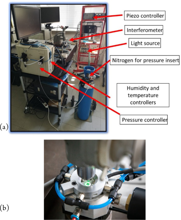
Advanced system with a second prototype environmental chamber: (a) microscope with T, P, and humidity control and (b) close-up of a Linnik head looking into the environmental chamber.
In a first prototype environmental chamber we succeeded in controlling the pressure of the nitrogen used to inflate the bubble (0–400 Pa) and the temperature (20 to 80 °C). We were also able to develop a successful protocol for the measurements which are not easy since at the nanoscale the sample moves with changes in pressure and temperature, requiring recentering of the measurements.
Nonetheless, a series of successful estimations were made of the creep compliance of polystyrene (PS) and poly(vinyl acetate) (PVAc) polymer films, showing that the transition temperature decreases for ultrathin polymer films compared with the values of the bulk material.8 A more advanced second prototype was then developed to include control of the humidity (Figure 8), using a controlled flow of humidified nitrogen over the sample, in front of the objective (Figure 9(a)).
Figure 9.
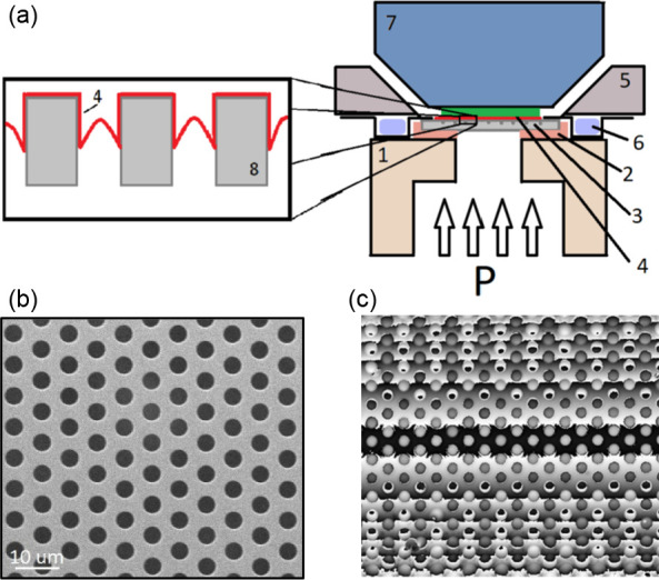
Details of a second prototype environmental chamber for the “nanobubble” technique. (a) Cross section of the experimental cell: (1) Teflon stand with a hole for the pressure input (P); (2) adhesive tab for fixing the sample and preventing leaks; (3) grid with holes; (4) ultrathin polymer film; (5) aluminum holder; (6) Peltier ring; (7) objective of interference microscope; (8) Si3N4 grid membrane with holes, (b) SEM image showing an array of closely spaced 5 μm diameter holes in the Si3N4 membrane, (c) unwrapped PSM measurement (with phase discontinuities) of surface height with interference fringes aligned along the y-direction of the holes in the grid after applying a pressure of 70 kPa.
The SEM image in Figure 9(b) shows the grid that consists of a regular array of 5 μm holes in a 0.9 μm thick Si3N4 membrane suspended on 0.4 mm thick Si support 5 mm × 5 mm in size (Aquamarijn MicroFiltrationBV, Netherlands). The polymer film is annealed at 40 °C to fix it in place, during which capillary forces draw it into the hole to a depth of approximately 200 nm.23 The environmental chamber was designed for use on a Leitz–Linnik interference microscope,8 positioned on the axial piezo table for phase stepping. Some typical results of the measurement of height using phase stepping are shown in Figure 9(c), the horizontal lines consisting of the typical phase discontinuities present for large heights which are left wrapped for the purposes of measurement precision. The interference fringes have been specifically aligned along the y-direction of the holes in the grid after applying a pressure of 70 kPa. Measurements of the profile of several bubbles are made along a line in the central region where unwrapping of the phase is unnecessary.
Some typical results of the evolution of the averaged profiles of a nanobubble of a PVac film at Texp = 63 °C are shown in Figure 10(a), the horizontal line at the bottom showing the bubble without pressure applied. The other curves are the bubble profile after applying a pressure of 0.7 atm and subsequent measurements taken periodically over a period of 3 h as the film relaxes. The average curvature and radius of the nanobubble are then measured at each point in time, and then the biaxial components of the stress σ and strain ε are estimated from the radius as a function of time.
Figure 10.
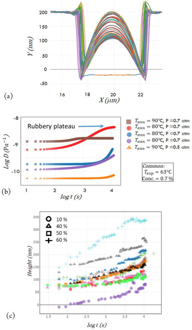
Results of advanced systems with a second prototype environmental chamber. (a) Example of evolution of bubble height with time over 3 h, at 0.7 atm and Texp = 63 °C. The colored curves are related to the time. (b) Plots of creep compliance over time. (c) Plots of height as a function of time showing strong correlation between humidity and creep compliance, leading to the conclusion that humidity acts as a plasticizer on PVAc films.
The Boltzmann superposition principle for a spherical sample is then applied to obtain the dynamic creep compliance D(t).23 Some typical results are shown in Figure 10(b) on log–log plots, the important feature to note being the appearance of the rubbery plateau under certain conditions, corresponding to the point when stress from the pressure is not enough to overcome the stress balance in the inflated film. The final results in Figure 10(c) show the change in height over time for different humidity levels from 10% to 60% humidity. The results show a strong correlation between the humidity level and the creep compliance values that proves the assumption that humidity acts as a plasticizer. The second prototype also allowed the study of the appearance of inflection in the evolution of the bubble shape in certain conditions. A first model of the bubble inflation was also developed using finite element modeling (the Marc and Mentat technique) in order to investigate the process of the bubble formation and growth and extract the mechanical properties of the film. This model could be improved in order to be able to study the creep and inflection behavior. Concerning the experimental work, further improvements could be made to the sample preparation, in automating the centering of the film position over time and in determining the variation of the thickness of the thin film during the experiment.
Measurement of the Drying Properties of Polymers Using an Automatic Dispenser of Microdroplets
The second system is being developed in the context of a project to develop a predictive simulation tool in order to describe the drying of complex waterborne colloidal formulations. In the well-known “coffee stain” problem, the formation of the resulting shape and size of the dry deposit from the liquid drop is complex.
The drying of the colloid layer depends on coupled phenomena of the transport of matter and heat, associated with stress build-up and relaxation over a wide range of characteristic length and time scales. Understanding the process is important in several fields where colloid drying is involved, such as in paints, cosmetics, glues, ink jet printing, pharmaceutical encapsulation, photonic crystals, or thin films in oxide fuel cells for example. To validate the assumptions underlying the simulations being developed, it would be useful to measure experimentally the profile of drying latex films, particularly near the drying front where the latex particles tend to agglomerate.
Measurement of the dry deposit is fairly easy (Figure 11(b)), showing some typical results made with a commercial Zygo NewView 7200 white light interferometer. Some tomographic measurements of water-based colloidal layers have previously been made using white light interferometry24 but were particularly difficult to measure because of the relatively high speed of evaporation of the droplet edge under the microscope.
Figure 11.
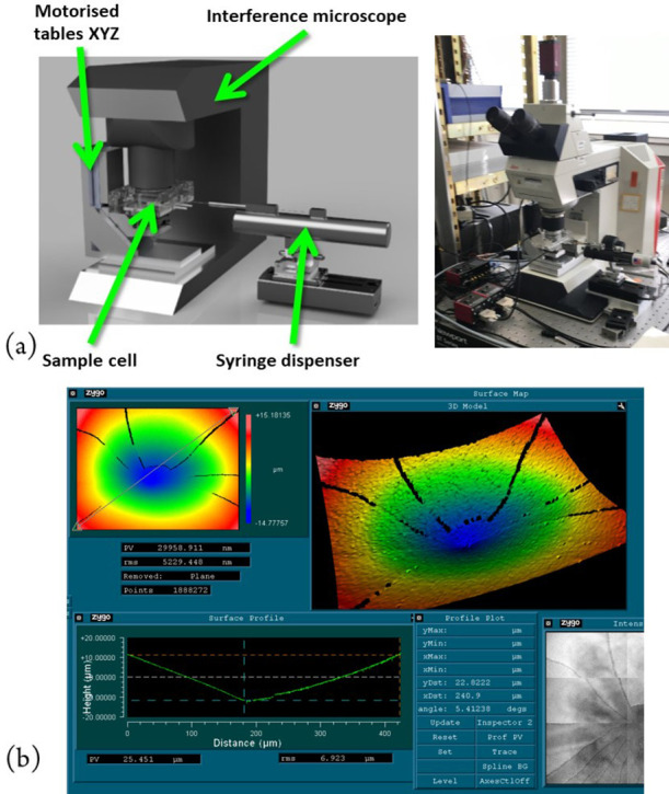
Automated microdroplet dispenser and microscope for measurement of evaporation of polymer microdroplets: (a) drawing of system layout and photo of microscope with an automated microdroplet dispensing system and (b) measurements with interferometry of the polymer after drying.
Manual coordination of the deposition of the droplet, focusing under the microscope, and then performing fringe scanning is in fact quite challenging. It was therefore decided to develop an automated droplet dispensing and measurement system using a motorized syringe dispenser and motorized translation stages to position the droplet under the interference microscope objective. The resulting system is shown in Figure 11(a). Some of the first tests were performed on a droplet of oil in order to test the system, a single set of measurements being shown in Figure 12.
Figure 12.
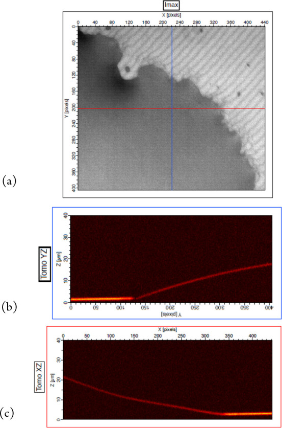
Measurement results of an automated dispenser system on a microdroplet of oil: (a) reflection image (Imax) showing a droplet on the left and substrate on the top right, (b) tomographic image (YZ) from the blue line in (a), and (c) tomographic image (XZ) from the red line in (a).
A high depth of field reflection image made by conserving the maximum intensities at each pixel can be seen in Figure 12(a), the darker area showing the droplet and the image size being 400 × 440 μm. Two measured profiles of the surface of the droplet are shown in Figures 12 (b) and (c). A single measurement involves acquiring typically 500 images which takes about 17 s using a grayscale Photofocus camera running at 30 i/s. A standard FSA algorithm is then employed to extract the profile data. In its present state, the system requires two PCs and two people to run the programs for controlling the microdroplet dispenser and making the interference measurement. A challenge also remains to increase the speed of measurement to be able to follow the change in the shape of the edge of the droplet as the liquid evaporates. Ideally, the dynamic range of measurement along the optical axis also needs to be higher, by several hundred μm. The system is being adapted to accommodate these new requirements. Another technique that can be used for studying droplet shape and wetting properties is reflection interference contrast microscopy (RICM), in which interferograms can provide profiles and even measurements of the surface deformation of liquid droplets resting on soft materials.25
Immersion System for Studying Changes in Colloidal Layers Immersed in Water
A final application of environmental chambers is the development of an immersion system for studying colloidal layers under a water flow containing pollutants in the context of the pollution of soils. Much research has begun in identifying changes in colloids due to their role and function in inhibiting environmental pollution of aquatic ecosystems, particularly in polluted urban rivers. The concept of a river health index system has received much attention by researchers and governments due to the correlation with human health and ecology. Rivers are often very close to the centers of human population and are at risk of being polluted from advanced industrialization which can worsen the availability of clean water and a healthy environment. Colloids have the capability of absorbing most of the trace metal fraction due to their high surface area. In other words, colloids, especially coarse or fine colloids (>1 μm or <900 nm), play a role in binding the pollutants.26
Because of their high roughness, colloids are known to be difficult to measure. One technique proposed is the use of transmission electron microscopy to investigate the statistical accumulation of the distribution of heavy metals and colloidal minerals in metal-contaminated lake sediments.27
One of our recent projects has been the development of an immersion Linnik microscope in collaboration with the IPHC (Strasbourg) with the goal of being able to characterize colloidal layers with white light interferometry subjected to a water flow containing contaminants such as heavy metals. The context of the project is within the study of pollution of the environment. A commercial Linnik microscope (Fogale Nanotech, France) has been modified and improved for use with immersion objectives, providing the advantage of being able to make measurements in water.
Moreover, both water immersion objectives are able to reduce light reflection from the sample surface and to minimize dispersion mismatch in the interferometer arms for depth scanning in transparent samples.13Figure 13 schematically represents the experimental setup of the microscope of a water-immersion Linnik head that uses water as a liquid medium in both the reference and object beam arms.
Figure 13.
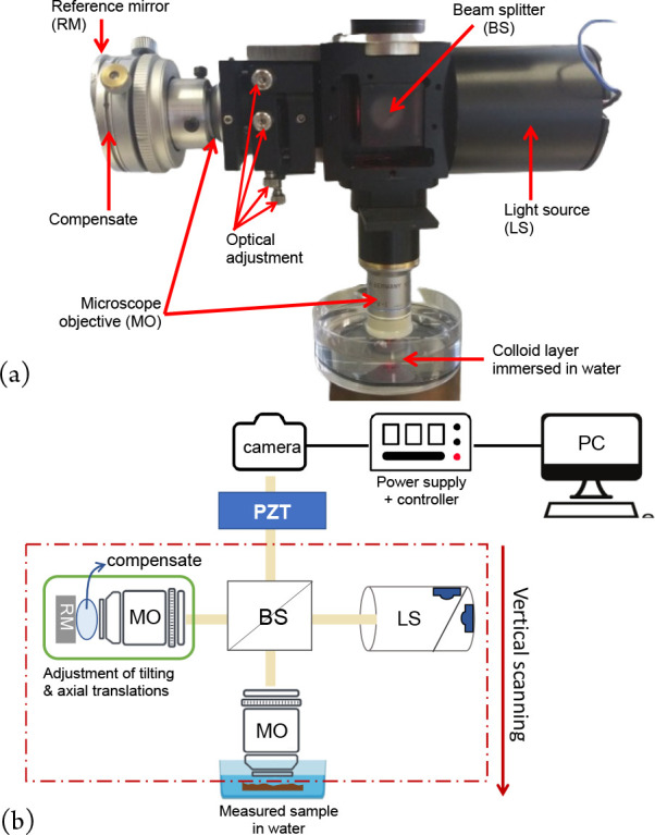
Immersion Linnik microscope for studying soil pollutants. (a) Details of Linnik head (installed at IPHC, Strasbourg) and (b) schematic layout of an immersion microscope with an SPA compensated reference arm.
A water-based compensator, sodium polyacrilate (SPA), was used in the reference beam arm due to the difficulty of using liquid water in the horizontal position of the reference arm.9 SPA was chosen because of its specific characteristics of being a nonliquid elastic polymer and the stability in its form at a maximum temperature of 25 °C. The refractive index of SPA is close to that of water, with a value of 1.335 as measured by an Abbe refractometer. In practice, we used an 8 mm diameter SPS hemisphere, with a thickness corresponding to the working distance of the objective and placed between the end of the reference objective and the reference mirror. The only inconvenience in using this material is the hemisphere needing to be changed after a few hours or days because of water evaporation.
To perform the CSI measurements, the sample is placed in a container filled with distilled water, and the piezo is used to move the interferometer head in order to scan the interference fringes over the full depth of the sample roughness. The illumination beam from a broadband white light LED at a center wavelength of 568 nm and spectral width of 100 nm at fwhm is split by a nonpolarizing cube beam splitter with R/T 45/45 for both arms.
The beams are then recombined by reflecting them back through the same beam splitter to the monochrome CMOS camera (Photonfocus MV1-D2048-96-G2 with 2048 × 2048 pixels, 22 fps) connected by a Giga Ethernet connection. The fringe envelope determination used is the FSA algorithm with π/2 phase steps. Some measurement results are shown in Figure 14, with false color images of the altitude data, the line profile of the surface, and a 3D image using Mountains Map v6 from Digital Surf. These results demonstrate the ability to measure topography in immersion conditions. The next step of the project will be to begin analyzing colloidal samples in immersion.
Figure 14.
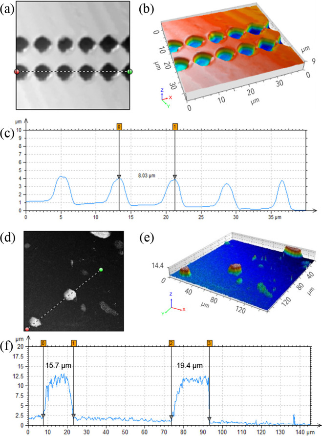
Results on etched squares in Si (6 μm wide, 2.5 um deep) measured with a ×20 water immersion Linnik system (NA = 0.5, λeff = 450 nm, working distance of 3.5 mm) and an aggregate layer of 1 g/L alumina measured with a ×40 water immersion Linnik system (NA = 0.8, λeff = 450 nm). (a) & (d) height images, (c) & (f) line profiles from (a) & (d), and (b) & (e) 3D images.9 Reproduced with permission from H. Mukhtar, P. Montgomery, F. Anstotz, R. Barillon, A. Rubin Immersion white light scanning interferometry using elastic polymer path length compensation. Proceedings of SPIE Photonics Europe, Optical Micro- and Nanometrology VII; 2018; Vol. 10678.9
Conclusions
Interference microscopy is a useful technique for characterizing functional materials, first providing rapid and quantitative measurements of microscopic surface topography. The main results of this review have shown how it is possible to considerably extend the number of characterization modes of the same system, to move toward multimodal microscopy, taking advantage of the specific properties of the interference optical probe used.
By using continuous fringe scanning combined with high-speed acquisition and processing with a high-speed camera associated with FPGA processing, it is possible to make 3D measurements in real time, with results being shown at rates up to 22 3D images per second. Such a mode is useful for measuring surfaces that are moving or changing continuously in an aperiodic way.
While single reflective surfaces give a single fringe signal along the optical axis for use in shape measurement, in the presence of a transparent layer, several fringe envelopes exist, each one corresponding to the different surfaces and buried structures and interfaces. Since the SNR of the signals is typically much lower than with just a single surface, various image acquisition and processing techniques are required to be able to usefully exploit the different signals, such as the use of “dark” and “flat” correction, the HDR technique, and image averaging. In this way, useful tomographic images can be made, with results being given of defects inside 6 μm thick polymer layers.
Because polychromatic light is used with interference fringes, by applying a Fourier transform to the fringe signal and suitable calibration of the optical system, local spectroscopy can be performed to measure the local optical properties over a small spot size, useful in the presence of inhomogeneous materials. The results are demonstrated on a Au layer on the Al substrate, producing a spectral cube from which the optical response can be presented at specific wavelengths over an area or as a function of the wavelength at specific points in the image. The technique can also be used for depth-resolved local spectroscopy of buried structures and interfaces by apodizing the different fringe signals over the optical axis. Other modes using the same data allow the local measurements of refractive index and thickness of transparent layers and the size measurement of individual spherical particles buried in a transparent layer.
To improve the lateral resolution for nanometrology with interference microscopy, a successful solution has been to combine a glass microsphere in the interferometer between the sample and objective. This allows the resolution to be improved at least 2-fold, although the field of view for a single measurement is reduced to about 1/5 of the diameter of the microsphere (typically between 20 and 150 μm).
Finally, three examples are given of the use of environmental chambers for measuring specific parameters under controlled conditions. The first one is for controlling the pressure, temperature, and humidity to measure the mechanical properties of nanometric polymer films, using the “nanobubble” technique. The second is a system for the automatic control of the deposition of microdroplets to measure the drying properties of polymers. The third is a specially developed immersion system that is planned to be used to study changes in colloidal layers immersed in water in the presence of heavy metals with an application in the study of pollution of the environment.
In this way, we have shown how the same interference microscope can be adapted to carry out multimodal microscopy useful for characterizing functional materials and systems.
Acknowledgments
The authors also wish to thank the staff from the C3Fab platform for helping with the sample preparation and characterization. Thanks are extended to Pierre Pfeiffer for help with the results in Figure 11(b).
Glossary
ABBREVIATIONS
- AFM
atomic force microscopy
- AD
aperture diaphragm
- CCD
charge-coupled device
- CMOS
complementary metal oxide semiconductor
- FPN
fixed pattern noise
- FSA
five-step adaptive
- fwhm
full width at half-maximum
- HDR
high dynamic range
- LED
light-emitting diode
- NCS
noncalibrated spectral response
- PS
polystyrene
- PSM
phase-stepping microscopy
- PRNU
photoresponse nonuniformity
- PVAc
poly(vinyl acetate)
- SEM
scanning electron microscopy
- SPA
sodium polyacrylate
- STF
spectral transfer function
Biographies
Paul Montgomery is a senior research scientist with the CNRS at the Engineering science, computer science and imaging laboratory (ICube) in Strasbourg, France. He received his Ph.D. degree in laser speckle instrumentation from Loughborough University, UK, in 1987. He has over 30 years experience in developing optical instrumentation for the characterization of materials and biomaterials. He is currently interested in label-free far-field nanoscopy, microsphere-assisted interference microscopy, local spectroscopy, and the use of environmental chambers for measuring specific parameters. He is a senior member of SPIE and a member of the Board of Directors of SPIE as well as a member of IOP and SFO.
Manuel Flury received his degree from the Ecole Nationale Supérieure de Physique de Strasbourg, France, his M.Sc. degree in Photonics, and his Ph.D. degree from Louis Pasteur University, Strasbourg, in 1998 and 2002, respectively. In 2002–2003, he was a Research Scientist in the Institute of MicroTechnology, Neuchâtel University, Switzerland. In 2003, he joined as Assistant Professor the Jean Monnet University, Saint-Etienne, France. Since 2013, he has been at the National Institute of Applied Sciences of Strasbourg, France, as an Assistant Professor and in the ICube Laboratory. He has coauthored 40 papers in international peer-reviewed journals and 80 contributions in international conferences.
Freddy Anstotz is an Assistant Professor at the University of Strasbourg and researcher at ICube Strasbourg. In 1991 he received his Ph.D. degree in electronic engineering and computer science from the University of Mulhouse. His main research interests are in the area of the development of digital electronics for mixed-mode electronics applied to sensors and real-time signal and image processing. He has been involved in several projects in ASIC design in collaboration with CERN or applied to medical X-ray readout electronics in mammography systems. Presently, his main work in the IPP group at the ICube laboratory is the implementation of algorithms on hardware or software platforms applied to interference microscopy.
Sébastien Marbach graduated from Télécom Physique Strasbourg Engineering School and received a M.Sc. degree in Photonics in 2018 from Strasbourg University. He defended a Ph.D. thesis in 2022 at the University of Strasbourg, concerning the development of interference white light microscopy for multimodal (spectral, colorimetric, and topographic) measurements. His personal interests are optical instrumentation, microscopy, nanoscopy, super-resolution, and optical metrology.
Christophe Cordier obtained the Diplôme Universitaire de Technologie from the University of Orsay, with a specialization in physical measurements (1995–1997). In 1997–2000, he obtained an engineering degree from CESI Ile de France, Bagneux, France, and worked at the Commissariat à l’Energie Atomique, Saclay, France, on a research team for the development of an atomic force microscope. Since 2004, he has been working at the National Institute of Applied Sciences of Strasbourg, France, as an assistant engineer and in the ICube laboratory. He is involved in the development of interferometric microscopes and several projects concerning instrumentation.
Jeremy Bartringer is an instrumental design engineer who has worked for 22 years with the CNRS and is presently in the ICube Laboratory in Strasbourg. He received an M.Sc. degree in laser physics and applications in 1999 and is currently specializing in laser and spectroscopic instrumentation for materials processing and characterization.
Husneni Mukhtar is a senior researcher–lecturer at the School of Electrical Engineering, Telkom Universit,y in Bandung, Indonesia, where she started her career after receiving her Ph.D. degree in electronics, microlectronics, and photonics from the University of Strasbourg, France, in 2018. She now supervises the laboratory of renewable energy and advanced electrical engineering (REAEE) in the Research Division of Control, Electronics, and Intelligent Systems (CEIS). Besides 3D optical profiling, her current main research interests are image processing instrumentation for inspection purposes in industry and analysis in the fields of biomedics and nanometrology. She also implements instrumentation and control in other application fields.
Audrey Leong-Hoï is a project manager in the field of e-health at GIP Pulsy, Strasbourg, France. She received her Ph.D. degree in electronics, microelectronics, and photonics from the University of Strasbourg in 2016, working on super-resolution in optical microscopy. Then, she worked on image processing and artificial intelligence algorithms in the medical field for three years. She is currently managing projects around dematerialized services for health institutions.
Anne Rubin is an Assistant Professor at the University of Strasbourg and researcher at the Institut Charles Sadron (ICS), Strasbourg. She is an engineer in materials science from E.N.S.A.M. (Ecole Nationale Supérieure d’Arts et Métiers, Paris, France) and gained her Ph.D. in 2006 in the study of DNA interactions using the coupling of electrochemical and acoustic techniques from the Université Paris 7, France. Her main research interests are in the areas of the study of interfacial shearing in multicontacts at the nanoscale, the shearing of molecularly thick layers (boundary lubrication), and the study of several material morphologies under contact confinement. She is presently interested in the nonlinear material properties of ultrathin viscoelastic polymer films.
Anastasiia Shpiruk obtained a Ph.D. degree in polymer physics in 2022 at the University of Strasbourg (France), where she studied mechanical properties of polymer films using a nanobubble inflation technique. Prior to that, she completed an international master program between France and Ukraine specializing in condensed matter, nanophysics, and medical physics where she investigated a process of supercoiling of DNA molecules by means of magnetic tweezers.
Mireille Delnero Del Nero is a senior scientist at the Hubert Curien Pluridisciplinary Institute (IPHC, CNRS – Strasbourg University) using (geo)chemistry to understand the migration behavior of radionuclides in natural systems. She has taken on major scientific challenges related to the field of environmental chemistry, i.e., molecular-level identification of chemical species, in situ speciation at (nano)mineral–solution interfaces, and complex natural organic matter, by using innovative experimental setups based on advanced surface spectroscopy techniques or on ultrahigh resolution mass spectrometry techniques. Her scientific expertise is applied to the fields of safety assessment of polluted areas or NORM (Naturally Occurring Material) or (Technologically Enhanced) NORM issues. She has been the scientific coordinator of the Radiochemistry group at IPHC and is senior member of the Steering Commitee of Long Term SocioEcological Research observatory on Uraniferous Territories.
Rémi Barillon is a professor at the Faculty of Chemistry at Strasbourg University and carries out his research activities at the Hubert-Curien Multidisciplinary Institute (IPHC, CNRS, and Strasbourg University). He completed his graduate studies at the University of Franche-Comté. After a stay of 16 months at the University of Exeter, he was then appointed lecturer in Strasbourg in 1996. He became a professor in 2006. His research activities concern the speciation of radioelements at the solid–liquid interface and chemistry under ionizing radiation. He is currently secretary of the international conference Nuclear Tracks and Radiation Measurements and deputy director of the Nuclear Sciences Research Group for Energy and the Environment (National Institute of Nuclear Physics and Particle Physics and National Institute of Chemistry of the CNRS). He is Vice President of Strasbourg University since April 2021 in charge of Research, Doctoral training, and Open Science.
Author Present Address
# Optiive, 300 Boulevard Sébastien Brant, Illkirch 67400, France
Author Present Address
¶ Telkom University, School of Electrical Engineering, Bandung 40257, Indonesia.
Author Present Address
⊥ PULSY, 2 rue Adolphe Seyboth, Strasbourg 67000, France.
Author Contributions
The manuscript was written through contributions of all authors. All authors have given approval to the final version of the manuscript.
This work received financial support from the ANR LatexDry project (AAPG 2018 – CES06), the University of Strasbourg, and INSA Strasbourg.
The authors declare no competing financial interest.
References
- Schmit J.; Reed J.; Novak E.; Gimzewski J. K. J. Performance advances in interferometric optical profilers for imaging and testing. J. Opt. A: Pure Appl. Opt. 2008, 10 (064001), 1–7. 10.1088/1464-4258/10/6/064001. [DOI] [Google Scholar]
- de Groot P.Interference Microscopy for Surface Structure Analysis. In Handbook of Optical Metrology: Principles and Applications; Yoshizawa T., Ed.; CRC Press: Boca Raton USA, 2015; Vol. 31, 791–828. [Google Scholar]
- Montgomery P. C.; Anstotz F.; Salzenstein F.; Montaner D.. Real time and high quality on-line 4D FF-OCT using continuous fringe scanning with a high speed camera and FPGA image processing. In Full-Field Optical Coherence Microscopy: technology and applications; Dubois A., Ed.; Pan Stanford Publishing: Singapore, 2016; 393–428. [Google Scholar]
- Leong-Hoï A.; Montgomery P.; Serio B.; Twardowski P.; Uhring W. High dynamic range microscope imaging based on exposure bracketing in full field OCT. Opt. Lett. 2016, 41 (7), 1313–131. 10.1364/OL.41.001313. [DOI] [PubMed] [Google Scholar]
- Marbach S.; Claveau R.; Wang F.; Schiffler J.; Montgomery P.; Flury M. Wide-field parallel mapping of local spectral and topographic information with white light interference microscopy. Opt. Lett. 2021, 46 (4), 809–812. 10.1364/OL.413036. [DOI] [PubMed] [Google Scholar]
- Leong-Hoï A.; Hairaye C.; Perrin S.; Lecler S.; Pfeiffer P.; Montgomery P. High resolution microsphere-assisted interference microscopy for 3D characterization of nanomaterials. Phys. Status Solidi A 2018, 215, 1700858 10.1002/pssa.201700858. [DOI] [Google Scholar]
- Perrin S.; Montgomery P.; Lecler S. Microsphere-assisted interference microscopy. In Roadmap on Label-Free Super-Resolution Imaging. Laser Photonics Rev. 2022, 10.1007/978-3-030-21722-8_17. [DOI] [PMC free article] [PubMed] [Google Scholar]
- Chapuis P.; Montgomery P. C.; Anstotz F.; Leong-Hoï A.; Gauthier C.; Baschnagel J.; Reiter G.; McKenna G. B.; Rubin A. A novel interferometric method for the study of the viscoelastic properties of ultra-thin polymer films determined from nanobubble inflation. Rev. Sci. Instrum. 2017, 88 (9), 093901 10.1063/1.5000948. [DOI] [PubMed] [Google Scholar]
- Mukhtar H.; Montgomery P.; Anstotz F.; Barillon R.; Rubin A. Immersion white light scanning interferometry using elastic polymer path length compensation. Proc. SPIE 2018, 10678, 10678L. 10.1117/12.2315474. [DOI] [Google Scholar]
- de Groot P. Principles of interference microscopy for the measurement of surface topography. Adv. Opt. Photonics 2015, 7 (1), 1–65. 10.1364/AOP.7.000001. [DOI] [Google Scholar]
- Marbach S.; Cordier C.; Claveau R.; Engel T.; Montgomery P. C.; Flury M. White light interference microscopy system design. Proc. SPIE 2020, 11352, 113521B. 10.1117/12.2555929. [DOI] [Google Scholar]
- Larkin K. G. Efficient nonlinear algorithm for envelope detection in white light interferometry. J. Opt. Soc. Am. A 1996, 13, 832–43. 10.1364/JOSAA.13.000832. [DOI] [Google Scholar]
- Dubois A.; Grieve K.; Moneron G.; Lecaque R.; Vabre L.; Boccara C. Ultrahigh-resolution full-field optical coherence tomography. Appl. Opt. 2004, 43, 2874–2883. 10.1364/AO.43.002874. [DOI] [PubMed] [Google Scholar]
- Fay M. F.; de Lega X. C.; de Groot P.. Measuring High-Slope and Super-Smooth Optics with High-Dynamic-Range Coherence Scanning Interferometry. In Classical Optics 2014, OSA Technical Digest (Optica Publishing Group), paper OW1B.3; 2014. 10.1364/OFT.2014.OW1B.3. [DOI]
- Leong-Hoï A.; Claveau R.; Flury M.; Uhring W.; Serio B.; Anstotz F.; Montgomery P. Detection of defects in a transparent polymer with high resolution tomography using white light scanning interferometry and noise reduction. Proc. SPIE 2015, 9528, 952807. 10.1117/12.2184559. [DOI] [Google Scholar]
- Fay M. F.; Dresel M. Applications of model-based transparent surface films analysis using coherence-scanning interferometry. Opt. Eng. (Bellingham, WA, U. S.) 2017, 56 (11), 111709 10.1117/1.OE.56.11.111709. [DOI] [Google Scholar]
- Claveau R.; Montgomery P.; Flury M. Spatially-resolved spectroscopic characterization of reflective and transparent materials at a micro-meter scale using coherence scanning interferometry. Phys. Status Solidi C 2017, 14 (11), 1700157 10.1002/pssc.201700157. [DOI] [Google Scholar]
- Claveau R.; Montgomery P.; Flury M.; Ferblantier G. Local inspection of refractive index and thickness of thick transparent layers using spectral reflectance measurements in low coherence scanning interferometry. Opt. Mater. (Amsterdam, Neth.) 2018, 86, 100–105. 10.1016/j.optmat.2018.09.046. [DOI] [Google Scholar]
- Claveau R.; Montgomery P.; Flury M. Coherence scanning interferometry allows accurate characterization of micrometric spherical particles contained in complex media. Ultramicroscopy 2020, 208, 112859 10.1016/j.ultramic.2019.112859. [DOI] [PubMed] [Google Scholar]
- Perrin S.; Li H.; Leong-Hoï A.; Lecler S.; Montgomery P. C. Illumination conditions in microsphere-assisted microscopy. J. Microsc. (Oxford, U. K.) 2019, 274 (1), 69–75. 10.1111/jmi.12781. [DOI] [PubMed] [Google Scholar]
- Boudoukha R.; Perrin S.; Demagh A.; Montgomery P.; Demagh N.-E.; Lecler S. Near- to Far-Field Coupling of Evanescent Waves by Glass Microspheres. Photonics 2021, 8 (3), 73. 10.3390/photonics8030073. [DOI] [Google Scholar]
- Hüser L.; Pahl T.; Künne M.; Lehmann P. Microsphere assistance in interference microscopy with high numerical aperture objective lenses. J. Opt. Microsyst. 2022, 2 (4), 044501–1. 10.1117/1.JOM.2.4.044501. [DOI] [Google Scholar]
- O’Connell P. A.; McKenna G. B. Novel nanobubble inflation method for determining the viscoelastic properties of ultrathin polymer films. Rev. Sci. Instrum. 2007, 78, 013901 10.1063/1.2409777. [DOI] [PubMed] [Google Scholar]
- Halter E.; Montgomery P. C.; Montaner D.; Barillon R.; Del Nero M.; Galindo C.; Georg S. Characterization of inhomogeneous colloidal layers using adapted coherence probe microscopy. Appl. Surf. Sci. 2010, 256, 6144–6152. 10.1016/j.apsusc.2010.02.019. [DOI] [Google Scholar]
- Mitra S.; Misra S.; Tran T.; Mitra S. K. Probing Liquid Drop Induced Deformation on Soft Solids Using Dual-Wavelength Reflection Interference Contrast Microscopy. Langmuir 2022, 38 (25), 7750–7758. 10.1021/acs.langmuir.2c00789. [DOI] [PubMed] [Google Scholar]
- Muirhead D.; Lead J. R. Measurement of the size and structure of natural aquatic colloids in an urbanised watershed by atomic force microscopy. Hydrobiologia 2003, 494, 65–69. 10.1023/A:1025481325455. [DOI] [Google Scholar]
- Togwell A.; Jackson M.; West M.; Leppard G. G. Accumulation and Partitioning of Heavy Metals by Bacterial Cells and Associated Colloidal Minerals, with Alteration, Neoformation, and Selective Adsorption of Minerals by Bacteria. In Metal-Polluted Lake Sediment. Geomicrobiol. J. 2011, 28 (1), 23–55. 10.1080/01490451003739406. [DOI] [Google Scholar]


