Abstract
Advances in flexible electronic devices and robotic software require that sensors and controllers be virtually devoid of traditional electronic components, be deformable and stretch‐resistant. Liquid electronic devices that mimic biological synapses would make an ideal core component for flexible liquid circuits. This is due to their unbeatable features such as flexibility, reconfiguration, fault tolerance. To mimic synaptic functions in fluids we need to imitate dynamics and complexity similar to those that occurring in living systems. Mimicking ionic movements are considered as the simplest platform for implementation of neuromorphic in material computing systems. We overview a series of experimental laboratory prototypes where neuromorphic systems are implemented in liquids, colloids and gels.
Keywords: artificial synapses, colloids, gels, ionic liquids, neuromorphic devices
A comparative analysis of the properties and materials of liquid, colloidal, and gel neuromorphic systems is presented. Various liquid‐based synaptic devices, as well as their neuromorphic applications, are also reviewed.

1. Introduction
Complex systems can be correspondingly abstracted in algorithmic formats to describe phenomena that have traditionally been cognition avoided. Such as the complexities of biological sensorial‐actuation networks, through which phenomena such as “intelligence” are hypothesized even in organisms without a nervous system. The sensor‐actuator collections represent the first order of cybernetic systems, which have been extensively studied and replicated. [1] Such applications of computational concepts and the development of experimental devices in that field enclasp “unconventional computing”.[ 2 , 3 ]
The term “neuromorphic” was invented by Carver Mead in the 1990s to refer to very large‐scale of integration computing systems (VLSI) with mixed analog/digital signals, inspired by the neuro‐biological architecture of the brain. [4] A neuromorphic feature of an engineered system mimics the structure or function of a single or multiple components of the Metazoan nervous system. Typically, this involves attempts to replicate the phenomenon of synaptic plasticity: self modulation of the excitability of neuron‐neuron junctions (synapses), towards replicating state retention (‘learning’) via a process of entrainment with graduated input (‘neuromodulation’). Neuromorphic devices, as an unconventional computational model, are worth researching owing to certain features of their biological counterparts, such as massive parallelism, emergence, and low power consumption, which are highly desirable for imitation.[ 5 , 6 , 7 , 8 , 9 , 10 , 11 , 12 , 13 ]
‘Neuromorphic engineering’ emerged as an interdisciplinary field of research that focusing on building electronic neural processing systems that directly imitate the biophysics of real neurons and synapses,[ 14 , 15 , 16 ] or ultimately allow direct communication with neurons. [17] Recently, the definition of the term neuromorphic has expanded in two additional directions. [18] Initially, the term neuromorphic was used to describe spike‐based processing systems that were engineered to discover large‐scale computational neuroscience models. Second, neuromorphic computations involve specific electronic neural architectures that implement neural and synaptic circuits. [19]
Neuromorphic computing hardware requires physical models at three different levels: (1) individual components such as artificial synapses and neurons, (2) Networks of these neurons and synapses, and (3) Learning rules and training methods. [20] Historically, early attempts at understanding the mammalian brain focused on the physical aspects of neurons including the McCulloch–Pitts neuron [21] and Rosenblatt perceptron, [22] which formed the basis for further development. Briefly, the cell body of a neuron collects and sums the charges generated by synaptic connections in the dendrites until the total charge reaches a threshold after which the neuron fires a spike along the axon. [23] The resulting spike is transmitted to other neurons connected to that synapse, which depending on the synaptic weight can augment or inhibit the signal. A more accurate Hodgkin‐Huxley physiological model [24] includes differential equations with more than 20 different parameters such as the concentrations of K+ and Na+ ions, which became the basis for subsequent approximations.[ 25 , 26 ] Subsequent research in neuroscience shifted the focus to the conceptual basis of higher levels of learning, cognition, and behaviour of neuronal populations, which the resulting models became the basis for Neural network architecture (ANN) (for example, Hopfield networks) and learning rules (for example, Hebbian learning). [27]
In this regard, systems such as Spiking Neural Networks (SNN), the third generation of neural networks, [28] are extremely representative. However, there is important cross‐fertilisation between the technologies needed to develop efficient SNNs and the more traditional non‐spiking neural network technologies, known as artificial neural networks (ANNs), which are usually time‐based. [29]
Early successes in neuromorphic computing have relied heavily on conventional electronic materials. In particular, spiking neural networks composed of silicon‐based Complementary Metal Oxide Semiconductor (CMOS).[ 30 , 31 , 32 ] Since CMOS chips have disadvantages such as inefficient and high energy consumption synaptic operations based on volatile random access memory (RAM), considerable effort has been focused on non‐volatile memory (NVM) as a basis for neuromorphic computing. [33] Among the empirical understanding of NVMs we should mention the Resistive Switching Devices (RSDs), to whom the memristors [34] belong, which has a transition between different impedance modes that can be related, for example, to binary information. Such a voltage‐controlled, reversible, stable transmission depends on several nano scale phenomena. [35] The simultaneous presence of NVM and multi‐mode switching in memristors[ 36 , 37 ] gives CMOS‐memristive hybrid circuits promising for edge computing and the Internet of Things, so that local processing of analog and digital data on mobile devices reduces the need for cloud access. [38]
Conventional Von‐Neumann computers based on CMOS technology do not have the inherent capabilities to learn or deal with complex data such as the human brain. [29] To overcome the limitations of digital computers, considerable research efforts have been made around the world to develop profoundly different approaches, inspired by biological principles. One such approach is the development of neuromorphic systems, namely computer systems that mimic the type of information processing in the human brain. [39]
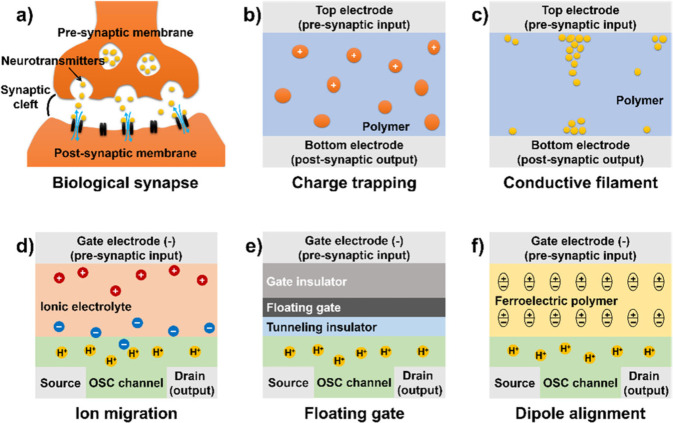
To mimic the synaptic functions of the brain, nonlinearity, memory features and rich systems dynamics are needed.[ 41 , 42 ] Dynamics, understood as evolution of systems in time (or time‐ordering of evolution steps) is the turning point of all neuromorphic computing systems. Exotic concepts, like time crystals (time crystal is a quantum system of particles whose lowest‐energy state is one in which the particles are in repetitive motion), [43] are considered as universal models for neuromorphic information processing. [44] This concept is fully in line with idea of polychronization: computation with spiking neurons operating in desynchronized fashion, thus forming a complex spatiotemporal fabric of oscillations [45] so important for cognitive processes. [46] One of the ways to achieve perfect mimicking of neuronal dynamics and information processing is replication of ionic movements in the nervous system (Figure 1). Therefore, it is important to note that ions move easily in liquids [47] and in soft matter in general. [48] Gels, viscous and non‐homogeneous media are especially interesting in this context ‐ complex diffusion and other transport phenomena, described in terms of fractional calculus, are ideal for mimicking complex dynamics of neural systems.[ 49 , 50 ] The term iontronics has been coined to describe electronic‐like devices and systems based on ion as information carriers. [51] In numerous cases iontronic devices are based on membranes with pores of controllable dimensions, which leads to anomalous transport phenomena.[ 52 , 53 ] These phenomena, in turn, embodied in devices called nanofluidic memristors, are proposed as a bio‐inspired information processing platform.[ 54 , 55 ]
Figure 1.
Schematic of (a) biological synapse, compared to organic artificial synapses with working mechanisms of (b) charge trapping, (c) conductive filament, (d) ion migration, (e) floating gate, and (f) dipole alignment. Reproduced with permission. [40] Copyright 2019, American Chemical Society (ACS) Publications.
Electrochemical process devices have shown promising synaptic properties that are useful in artificial synaptic devices because the electrochemical reactions of ions can mimic the movement of ions in the nervous system.[ 56 , 57 ] Along with synaptic functionalities, interaction of metal ion with neural extracellular matrix in the brain was postulated to be responsible for metal, most probably via modulation of synaptic plasticity. [58] Resistive switching and extremely fast (at least as compared with living neurons) responses up to the range of hundreds of kHz have been observed in electrochemical devices, which allow the expansion of biological functions. [59]
The Liquid State Machine (LSM) [60] is a nervous system‐inspired algorithm that mimics the brain's ability to process spatio‐temporal data. Of course, this particular term ‘liquid’ does not mean that the physical system is in a liquid state, but rather refers to the surface of a liquid that is affected by input forces and creates a pattern of reciprocal waves. A single LSM network can be used as a general intelligent processor that processes different data streams on a single stream to extract different features. [61] The flow of the LSM model training process is as follows:
Initialization. Each neuron in the fluid is randomly selected as an inhibitor or excitator, depending on the ratio of inhibitory or excitatory neurons. The entire set of connections and their corresponding synaptic strengths are initialized.
A set of inputs u(t) are fed into the input layer.
The liquid response is calculated based on step (1).
The responses in the previous time step are fed into the output layer and are also stored for the next time step (to calculate liquid response).
The Liquid response is used to train the next category, using a specific training algorithm and update rule.
Repeat steps 2–5 on all of the input training sets. [61]
The liquid state machine (LSM) [60] mimics the cortical columns in the brain. Cortical microstructures are thought to represent non‐linearly input stream into a high‐dimensional state space. This high‐dimension representation is then used as input to other areas in the brain where learning is possible. The cortical microcircuits have a sparse representation and (slowly) fading memory. The microprocessor state is in the ‘forgets’ state for a certain period of time. While LSMs may be able to mimic certain functions in the brain, it should be noted that LSMs cannot be used to explain how and why the brain functions. [62]
Liquid marbles (LMs) are spherical microlitre quantities of fluid with a coating of superhydrophobic particles that can be tens to thousands of micrometers in diameter.[ 63 , 64 ] LM devices are able to perform computation through a variety of non‐standard logics, where the LMs are considered as data or otherwise, to contain data (i. e. chemical reactants), which may interact with other LMs via collisions that will result in data translation or transfer via ricochets or coalescence.[ 65 , 66 ] By exploiting the principles of collision‐based computing, [67] LM computing devices may be used to implement non‐standard, collision‐based conservative logic. [68] The integration of LM properties, such as collisions that their results may have been engineered (reflection or integration), and the potential for chemical reactions between two heterogeneous fluid cores after collisions, further reinforces the traditional conservative logic toolkit. [13]
In the present review, we first briefly introduce the liquid, colloidal, and gel neuromorphic systems, followed by the review of various liquids, colloids and gels synaptic devices and their achieved results in neuromorphic computing.
2. Neuromorphic Liquid Systems
In abstract neural networks, information is displayed as weighted connections or synapses between neurons (Figure 2). Since the primary computational bottleneck for artificial neural networks is multiplication of the matrix vector so that the inputs are multiplied by the weight of the neural network, conventional processing architectures are not suitable for simulating neural networks and often require a lot of energy and time.In addition, in biological neural networks, synapses are not binary junctions, but represent a nonlinear response function because neurotransmitters propagate between neurons. [62] Synapse like liquid devices are summarised in Table 1, in the following we discuss some of the key implementations.
Figure 2.
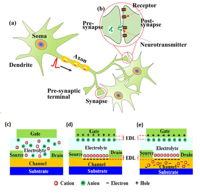
(a) Schematic diagram of a biological neuron. (b) Schematic illustration of a biological synapse. (c) Structure diagram of a top gate electrolyte‐gated transistor (d) Schematic diagram of the EDL modulation of the electrolyte‐gated transistor. (e) Schematic diagram of the electrochemical modulation of the electrolyte‐gated transistor. Reproduced with permission Copyright. [69] 2021, American Institute of Physics (AIP).
Table 1.
Summary and comparison of reported synaptic neuromorphic liquid devices.
|
Neuromorphic liquid device |
Device materials |
Availability of stimuli |
STP/STD |
LTP/LTD |
Functionality of plasticity |
Refs. |
|---|---|---|---|---|---|---|
|
MoO3 device |
2D MoO3 |
Electricity |
No |
No |
yes |
[70] |
|
Memtransistor |
2D SnO2 |
Electricity |
yes |
yes |
yes |
[71] |
|
Transistor |
PDVT‐10, Ion gel, Si |
Electricity |
yes |
yes |
yes |
[72] |
|
Flexible RRAM |
PEDOT:PSS |
Electricity |
yes |
yes |
yes |
[73] |
|
Transistor |
PEDOT:PF6 |
Electricity |
yes |
yes |
yes |
[74] |
|
Memristor |
Cu/Ag@AgCl |
Electricity |
No |
No |
yes |
[75] |
Neurons regulate synapse weight depending on stimulation to store information, and neuromorphic computational concepts use “synaptic plasticity“ to mimic short‐ and long‐term memory processes. Inspired by this, Cheng Zhang's group [70] have presented a systematic study of ionic liquid gating of exfoliated 2D molybdenum trioxide (MoO3) devices and the resulting electrical properties by electrochemical doping through ion migration during ionic liquid bias (IL) Related. The formation of a dual electrical layer in ionic liquid (IL) can induce charge carriers electrostatically or collect ions inside and outside the lattice. This process can cause many changes in the electronic, optical and magnetic properties of the material and even change the crystal structure of the material. In this study, the conductivity of the MoO3 was approximately 9‐fold for the two types of ionic liquids studied. In addition, it was possible to turn on and off quickly through a lithium‐containing ionic liquid, while much slower fusion was induced through oxygen extraction. [70]
In this study, the positive IL gate voltage increased the conduction of the channel and was attributed to an cation that reacted with H+ to form a hydroxyl (OH−) bond and at the same time change the capacitance of to valence change, thus electron doping the conduction band. Negative gate bias (at higher voltages) reduced channel conduction and was attributed to H+ removal through OH− accumulation in the channel. Because the team measured the vacuum, they suggested that the change in conductivity in MoO3 was due to the migration of oxygen in and out of the MoO3 through the IL gate. The data show that the process of metallization (production of oxygen vacancy) was faster than the reversible process (oxygen extraction). [70]
In this study, they used gate pulses as a stimulus to regulate the drain current (I d ) which acts similar to a synaptic memory process. Short and long‐term memory can be adjusted by tuning the drain voltage, and long‐term memory signal intensity can be adjusted by the gate pulse width. At 1 V sd , the current (I d ) changes after each pulse, which in neuromorphic calculations is referred to as the “excitatory postsynaptic current”. These MoO3 ions with Lithium Ion Liquid (LIL) devices can detect a long‐term current (I d ) change from nA to μA through short pulses. Each of these devices can function as a single unit and can be turned into a network to store information in a non‐volatile manner. The results of short pulse experiments in this study also show synaptic plasticity for computational neuromorphic elements. [70]
In a new study, an integrated device of a memristor and a transistor containing a new type of gate adjustable memristor based on the two‐dimensional SnO2 semiconductor was proposed by Chi‐Hsin Huang and colleagues [71] to advance the next generation of neuromorphic computing technology. An oxide memristor with an tunable gate was developed using SnO2 atomic ultra‐thin polycrystalline nanosheets with a thickness of about 2 nm, which is energy efficient and can be used in next generation neuromorphic computational applications.
2D‐SnO2 polycrystalline memristors, obtained at low temperatures from a vacuum‐free liquid metal process, offer several interesting resistive switching features such as excellent digital or analog resistive switching, multi‐mode storage, and gate adjustment performance in resistive switching modes. Significantly, the gate tunability function that is not achievable in conventional two terminal memristors provided the capability to perform heterosynaptic analog switching by adjusting the gate bias to enable complex neural learning. They have successfully demonstrated that the gate‐tunable synaptic device dynamically modulated the analog switching behaviour with good linearity and an improved conductance change ratio for high recognition accuracy learning. [71]
Artificial neural network simulations for pattern recognition were obtained with high detection accuracy in gate‐adjustable SnO2 two‐dimensional memristors. In addition, the presented planar 2D‐oxide memristors with very low conductivity consume very little energy and have the high potential to develop as an energy‐efficient biological nervous system, such as the human brain. The gate‐adjustable 2‐dimensional oxide memetransistor presented in this report improves detection accuracy and develops neuromorphic devices that mimic multiple synaptic connections in neurons. It also opens up new opportunities for designing learning schemes with a greater degree of freedom. [71]
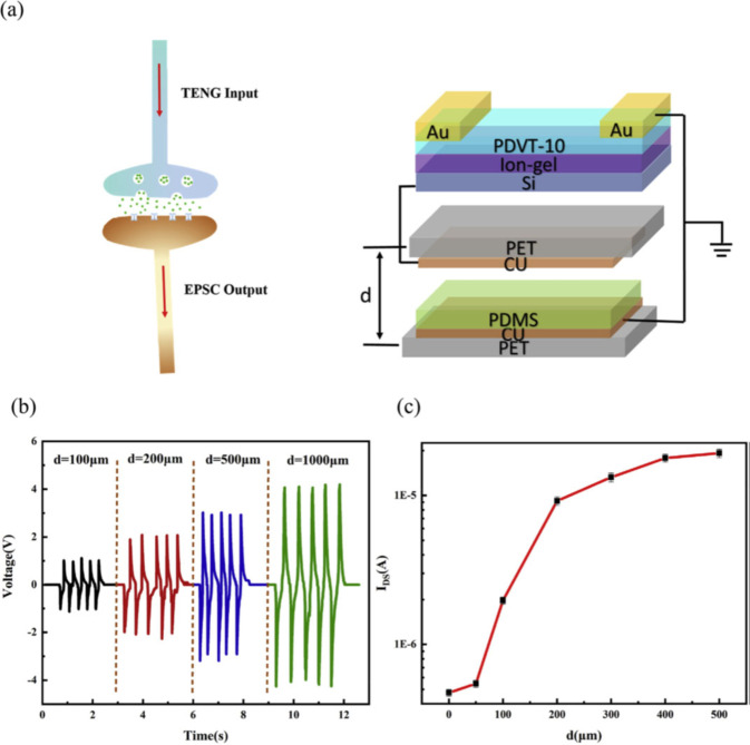
Artificial synapse devices with low energy consumption are very desirable to imitate the human brain. Thus, Yaqian Liu's team [72] developed a self‐powered synaptic transistor (SPST) with a distinct structure to simulate synapse functions. The voltage required for this transistor to produce a presynaptic spike is supplied by a triboelectric nanogenerator (TENG), without the use of additional voltage. The proposed SPST device consisted of a TENG with PET/Cu/PDMS/Cu/PET structure as a presynapse stimulation, and the channel between source and drain electrode in electric‐double‐layer (EDLT) was presented as post‐synapse. A schematic of the structure of a typical biological synapse and self‐powered synapse transistor (SPST) device is shown in Figure 3.
Figure 3.
(a) Schematic illustration of a biological synapse and the SPST. Touch bottom TENG will produce a pre‐synaptic spike to the gate to achieve a self‐powered synapse. (b) Open‐circuit voltage (Voc) with varying separation distances. (c) IDS‐d transfer characteristic curve of the SPST. Reproduced with permission. [72] Copyright 2019, Elsevier.
The presynaptic spikes of this device, unlike standard synapse devices, were generated by external mechanical contacts, resulting in a considerable reduction in synapse device power usage. Observations revealed that the artificial synapses performed well with varying touch spike duration times, and that with increasing stimulation, a short‐term plasticity transition to a long‐term plasticity occurred. Furthermore, combining TENG and a synapse device might successfully simulate tactile synapse functions while consuming insignificant power and having a basic device architecture. In addition, self‐charging synaptic devices with several TENGs understood logic modulation and tactile investigation. [72]
The TENG can also serve as a tactile sensor, allowing for the creation of a self‐charging tactile synapse device with a basic form. With the use of TENG touch, important synaptic functions such as excitatory postsynaptic current (EPSC), paired‐pulse facilitation (PPF), dynamic filtering, and short‐term plasticity (STP) to long‐term plasticity (LTP) were demonstrated in self‐powered synaptic transistor devices. A tactile study was replicated using TENG as multiple presynaptic, and logic gates were derived by using and, and or logic gates. Integrating TENG and synapse transistors is a promising approach for artificial intelligence and human‐computer interaction in e‐skin devices. [72]
A flexible artificial synaptic device with an organic functional layer was proposed by Tian‐Yu Wang and colleagues. [73] They created a flexible RRAM out of PEDOT : PSS and investigated its current response to various voltages. Under direct‐current sweep, the device demonstrated excellent resistive switching characteristics. At low operation voltages, it switched from high resistance state (HRS) to low resistance state (LRS) and back to HRS. Also, this organic device demonstrated good switching characteristics, such as an ON/OFF ratio greater than 100. The set and reset voltages were less than 0.5 V and 0.25 V, respectively. This flexible synaptic device was used to mimic long‐term plasticity, spike‐timing‐dependent plasticity learning rules (STDP), and forgetting function. Both the excitatory and inhibitory post‐synaptic currents had retention times greater than 60s. The long‐term plasticity without significant degradation was reproducible after applying five cycles of voltage pulse to the upper electrode. [73]
The synaptic device developed in this study had a structure of Indium Tin Oxides (ITO)/PEDOT : PSS/Au with a cross‐sectional junction circle of 200 um diameter, as shown in Figure 4. Polyethylene terephthalate (PET) was adopted as the flexible substrate. The electrode of Au was deposited on PEDOT:PSS with a shadow mask by physical vapour deposition. The controllable conductivity in this device was related to the transformation and migration of PEDOT+ ions. [73] This team applied voltage to the top electrode and recorded the responded current of the bottom electrode to to evaluate the device's characteristics. After five repeatable experiments with 300 positive and 300 negative pulses for LTD and LTP, no obvious degradation was observed in the device. These results demonstrate the feasibility of RRAM‐based organic PEDOT:PSS flexible bi‐terminal, which is used as artificial synapses for neuromorphic calculations and has great potential for wearable electronics applications (Figure 4). [73]
Figure 4.
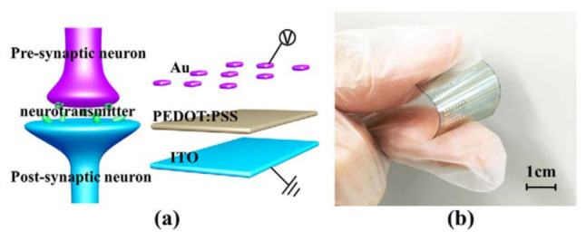
(a) The schematic structure of a bio‐synapse and the corresponded PEDOT:PSS‐based RRAM; (b) optical image of our flexible synaptic device in the bend state. Reproduced with permission. [73] Copyright 2018, MDPI Publications.
There was also an exploration of the space parameters of soft NV RSDs by using flexible polymers and the chemistry of Ag ions and nanoparticles, leading to several interesting results, in particular: a stability to cycling above cycles with the system based on AgNO3, PVDF‐HFP and ionic liquid, having ON/OFF ratio around 10 and a retention time in the order of 1000 seconds; [48] a maximum ON/OFF ratio above for systems based on AgNO3, PEO and ionic liquid, leading to cyclic stability around 500 cycles and retention time above seconds; [35] the formulation of a printable ink leading to a Write Once Read Many (WORM) flash memory. [76]
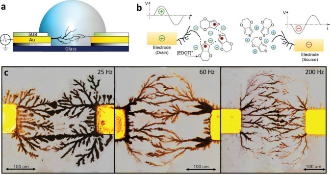
An emerging class of devices, organic electrochemical transistors (OECTs), operate in electrolyte solutions and exhibit controllable memory effects, holding great promise for bioelectronics and neuromorphic computing. In a study, Matteo Cucchi's group [74] have proposed AC‐electropolymerization to produce directionally controlled channels (Figure 5). Through changing the polymerization parameters, including voltage, frequency, and salt concentration, it is possible to adjust physical properties such as strength and capacitance. [74]
Figure 5.
Set‐up and growth of the dendritic networks. a) Setup and materials used to grow the organic dendritic networks. b) Sketch of the polymerisation process: during the positive polarity of the applied electrical signal, the anions oxidise the monomers at the interface and trigger the reaction; during the negative polarity, the monomer surrounded by cations is inert. c) Networks grown at 4 V with varying frequency: higher frequencies promote thinner fibres and a higher degree of bifurcation. Reproduced with permission. [74] Copyright 2021, John Wiley & Sons
The monomers used in this research was 3,4‐ethylene‐dioxythiophene (EDOT) and the salt was tetrabutylammonium hexafluorophosphate (TBAPF6). TBAPF6 is not only a suitable salt with high potential for electrochemical processes, but also an oxidizing agent for the monomer and an efficient dopant for the polymer derived from polymer poly(3,4‐ethylenedioxythiophene)‐tetrabutylammonium hexafluorophosphat. Conductive fibers of poly‐3,4‐ethylenedioxy‐thiophene doped with hexafluorophosphat (PEDOT:PF6) were prepared by AC electropolymerization in an electrolyte solution under AC signals (square wave 10–200 Hz) with between two gold electrodes.
Polymerization was carried out in three steps: [74]
By introducing a positive voltage above the monomer oxidation potential, the radicalization at the electrode/electrolyte interface was motivated. An electrical double layer (EDL) was formed as (PF) anions drifted to the electrode and accumulated.
An anion neutralized the radical cation of EDO .
The EDOT:PF6 complex had now reached a state of neutrality and was reacting with other EDOT
An almost isotropic growth would be induced by DC voltage, resulting in a closed film covering the entire positive bias electrode, expanding in any direction which was inconvenient for transistor channels. However, this study found that an AC stimulus (square wave, duty cycle 50 %) caused the little amount of polymerization only where the kinetics were fast. Fibers prefer to grow in areas where the local field is higher since the reaction rate depends on the concentration of anion. By growing new fibers, the field would become stronger in the next cycle (tip effect), and would accelerate reactions at the end of the fiber rather than the base (Faraday cage). Furthermore, an AC stimulator enables growth in a selectable spatial direction to bridge two or more electrodes on the substrate, allowing the channels to be upgraded multiple times. [74]
For neuromorphic applications, the growth method proved highly valuable since it allowed for the fabrication of devices that followed learning principles with arbitrary time constants. Adjustable neuromorphic features and the ability to decrease channels to the micrometre size were used to highlight the advantages of this technique. Finally, they address the issue of miniaturisation by demonstrating sub‐micrometer devices integrated in a dense crossbar array on a flexible substrate. [74]
Soft memory devices for smooth nerve transmission, as well as wearable applications, attract a lot of attention due to the ion concentration polarisation mechanism. [77] Muhammad Umair Khan and his colleagues, [75] proposed a core‐shell soft ionic liquid (IL)‐resistive memory device, using Cu/Ag@AgCl/Cu for electronic synapses. Cu ions were significantly controlled in the liquid electrolyte by the Ag@AgCl core‐shell, leading to a multi‐state resistive switching characteristic.
According to Figure 6, the core shell‐based device was strongly affected by the polarization of ion concentrations, which is the main cause of synaptic activity. The pulse width, frequency, and amplitude of pulses were studied in both positive and negative voltage regions. It was discovered that the core‐shell IL soft memory device could open a gateway for electronic synapses by demonstrating stable synaptic behavior in bending tests. [75]
Figure 6.
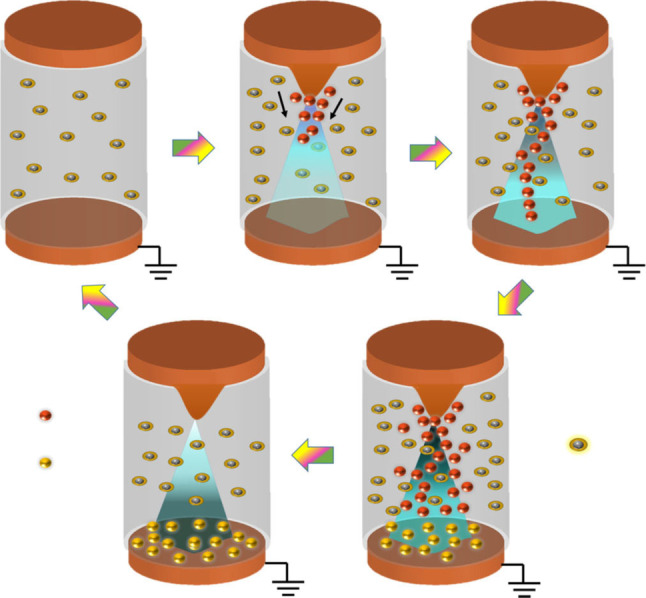
Proposed model for working mechanism of the artificial synaptic device using Ag@AgCl core‐shell ionic liquid. The working mechanism of the core‐shell soft ionic liquid neuromorphic device. Reproduced with permission. [75] Copyright 2021, Nature Publishing Group.
3. Neuromorphic Colloid Systems
The reported synapse like colloid devices are summarised in Table 2. The first study to demonstrate liquid state, colloidal RSDs goes back to 2016. [82] Chiolerio and co‐authors showed that ZnO nano and microparticles can be used to create flexible soft RSDs after photocuring, or liquid devices when the system is still at liquid state, prior to curing. Comparing the degree of polymerization, from the null state (oligomer, liquid state) to the soft crosslinking to strong crosslinking, the oxidation state at the particle surface (including a range of positions from the metal state to the variable oxygen vacancy density), and the degree of interaction between Oxygen vacancies and ethoxylated groups, it was possible to adjust the electronic properties of the obtained devices. A new interaction mechanism called the interfacial coupling mechanism (ICM) was developed.
Table 2.
Summary and comparison of reported synaptic neuromorphic colloid devices.
|
Neuromorphic liquid device |
Device materials |
Availability of stimuli |
STP/STD |
LTP/LTD |
Functionality of plasticity |
Refs. |
|---|---|---|---|---|---|---|
|
Sodium ion reservoirs |
Na2TP@Nafion |
Electricity |
yes |
yes |
yes |
[47] |
|
Memristor |
CNT‐Cu |
Electricity |
No |
No |
No |
[13] |
|
Optoelectronic device |
Si−Si nanocrystals |
Light |
yes |
yes |
yes |
[78] |
|
Photoelectrochemical synapse |
CdS/MWCNT composites |
Light |
yes |
No |
yes |
[79, 80] |
|
Transistor |
LiCoO2/SrTiO3 |
Electricity |
No |
yes |
No |
[81] |
In one study, Dongshin Kim et al., [47] demonstrated the use of [Na+] cations in an aqueous solution to transmit electrical signals, as liquids can be useful components for neuromorphic devices. By utilizing ion reservoirs for synaptic properties, they developed a neuromorphic device that controlled [Na+]. Schematic of the device structure is shown in Figure 7. According to the applied stimuli, NaCl‐based device exhibited synaptic characteristics of potentiation, depression, STP, LTP, and STDP. Electrochemical reactions between [Na+] and Na2TP@Nafion were used to simulate the signal transmission processes of neurons. To control synaptic properties and simulate synaptic functions, the device used an aqueous solution of [Na+].
Figure 7.
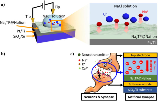
Schematic device structure and biological synapse. a Left side: Structure of the device, consisting of a Pt bottom electrode, a Na2TP@Nafion layer, a NaCl solution, and a top electrode; Right side: Detailed schematic showing ions in the NaCl solution on the surface of the Na2TP@Nafion layer. b Chemical structure of Na2TP and insertion or removal of Na+. Comparison of a biological synapse and an artificial synapse. Reproduced with permission. [47] Copyright 2020, Nature Publishing Group.
To control the concentration of [Na+] in the liquid, sodium terephthalate (Na2TP) was used as a reservoir. The device's synaptic functions were then induced by a change in [Na+]. potentiation, depression, excitatory postsynaptic current (EPSC), paired‐pulse facilitation (PPF), and spike timing‐dependent plasticity (STDP), were all observed in the device. The device operated in four distinct states. In the beginning, [Na+] and [Cl−] were distributed randomly in the NaCl solution. Nafion separates the NaCl solution and Na2TP. In the initial state, [Na+] and [Cl−] could be displaced by bias polarity when positive bias pulses were applied to the device.
With repeated stimulation, the ionic current gradually decreased due to the ion diffusion characteristics in the solution. [Na+] could not be absorbed in the Na2TP if the applied voltage was low. As a result, the [Na+] in the solution remained unchanged, and the device's conductivity returned to its original level. When a high enough voltage was supplied, [Na+] was able to pass through Nafion and react with Na2TP. The [Na+] was subsequently absorbed into the Na2TP, lowering the [Na+] in the solution and decreasing the device's conductivity. The Na2TP could release the [Na+] absorbed in it when a negative voltage was applied to the device. The applied negative voltage increased the concentration of [Na+] in the solution, resulting in potentiation. The [Na+] in the solution could be controlled by the number and amplitude of bias pulses. These EIS results could be used to calculate ion mobility and concentration. The diameter of the semicircles altered as a result of the reaction between Na2TP and [Na+] during the bias voltage was applied. [47]
Richard Mayne and his colleagues [13] fabricated liquid marbles with neuromorphic properties through copper coatings and fluid cores containing carbon nanotubes 1 : 0 mg ml−1. The experiment was performed by sandwiching marbles between two cup electrodes and stimulating them with repeated DC pulses at 3 : 0 V.
This study was presented as a pathway for the development of microlitre‐quantity three‐dimensional ballistic‐chemical reactors, which exhibited neuromorphic properties and may hence be used as unconventional computing media. Their results demonstrated that entrainment copper liquid marbles filled with carbon nanotubes can cause their electrical resistance to change rapidly between high to low resistance profiles, through periodic pulses, upon inverting the polarity of stimulation. The advantages of their devices, which are enclosed in liquid marbles, are enormous, but revolve around soft and ballistic data sources, the contents of which may be considered as chemical reactors. This technology is of interest to the design and fabrication of massively parallel wet computers, which include their applications from computing to biomedicine. [13]
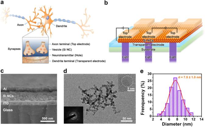
In another research, Hua Tan and colleagues [78] used Si−Si nanocrystals (NCs) to make synaptic devices, which could be effectively illuminated by light over an unprecedented region of the ultraviolet to near‐infrared spectrum, which has a wavelength of about 2 micrometers. These Si‐NC‐based synaptic devices with optical stimulation demonstrated a series of important synaptic functions that mimicked biological synapses well. Figure 8 schematically shows a biological neural system with typical synaptic structures and the structure of an array of Si‐NC based synaptic devices.
Figure 8.
Biological and Si‐NC‐based synapses. (a) Schematic of biological neurons that are connected with synapses. (b) Schematic of an array of Si‐NC‐based synaptic devices. The top electrode, Si NCs and transparent electrode represent the presynaptic axon terminal, vesicle and postsynaptic dendrite terminal, respectively. Stimulus light is introduced from the transparent‐electrode side. (c) Cross‐section SEM image of a Si‐NC‐based synaptic device. The thickness of the Si‐NC film is about 300 nm. (d) Low‐resolution TEM image of Si NCs. The selected area electron diffraction (SAED) and high‐resolution TEM image are shown as the insets. (e) Size distribution with a log‐normal fit for Si NCs. The mean size of B‐doped Si NCs is about 7.5 nm. Reproduced with permission. [78] Copyright 2018, Elsevier.
In this work they have used highly boron‐doped Si NCs to fabricate optically stimulated synaptic devices. The plasticity of Si‐NC‐based synaptic devices originated from the dynamic entrapment and propagation of photogenerated carriers at defects such as dangling bonds at the NC surface. When pulsed optical signals in the wide UV to NIR region were used as input spikes, these Si‐NC‐based synaptic devices performed important synaptic functions such as excitatory postsynaptic current (EPSC), paired‐pulse facilitation (PPF), short‐term plasticity (STP) to long‐term plasticity (LTP) transition and spike‐timing‐dependent plasticity (STDP). It was found that the performance of the device is mainly controlled by the electronic and optical behavior of Si NCs. The current ease of use of Si NCs in broadband, low‐energy consumption optoelectronic synaptic devices has important implications for large‐scale Si use in emerging neuromorphic computing. [78]
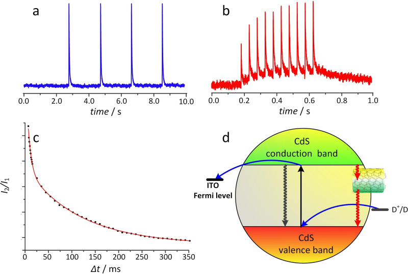
Plasticity of photoelectrochemical responses have been observed in CdS‐multiwalled carbon nanotubes composites [79] as well as tetragonal (hawleyite) and hexagonal (greenockite) polymorphs of cadmium sulfide. [80] Stimulation of photoelectrodes fabricated with one of the above mentioned materials on flexible substrates ((poly)ethylene terephthalate foil coated with indium‐doped tin oxide) in the presence of liquid or gel electrolytes resulted in photo‐current responses that can be described as spike‐rate dependent plasticity: the amplitude of photo‐current pulses increased with the number of light pulses applied and also with decreasing time interval between pulses (Figure 9).
Figure 9.
The response of the artificial synapse upon illumination (450 nm) with (a) 2 s and with (b) 50 ms time intervals between light pulses. The plasticity of the studied synaptic system with the fit line described by bi‐exponential function (c) The charge trapping mechanism responsible for the synaptic behavior of the CdS/MWCNT‐based device. Reproduced with permission. [79] Copyright 2020, John Wiley & Sons.
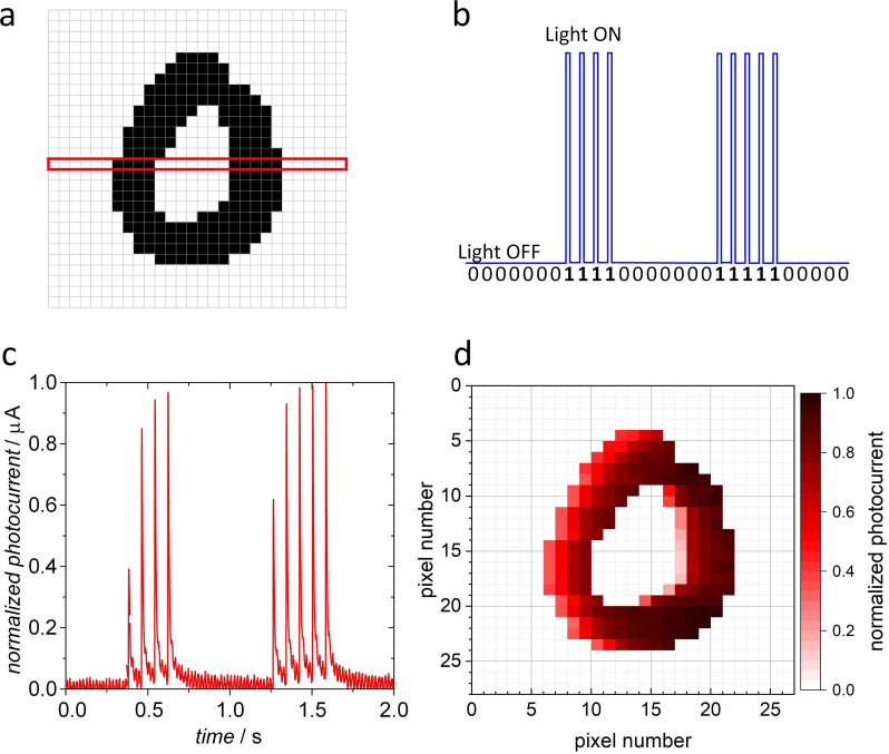
Observed synaptic plasticity is a result of two competing secondary processes following charge‐carrier generation: interfacial charge transfer (blue arrows in Figure 9d) and charge trapping (red arrows in Figure 9d). Due to significant difference of reaction rates, filling the trap states associated with carbon nanotubes, result in gradual increase in photocurrent amplitude. E excitation of CdS nanoparticles occurs results in the generation of electron–hole pairs, which undergo subsequent dissociation under the influence of internal electric field and give rise to photo‐current spikes, however their intensity is decreased by parasitic processes of charge trapping and charge carrier recombination. In the case of long‐lived charge trap states the intensity of subsequent photocurrent pulses increase due to gradual filling of the trap states. Therefore, in the case of short intervals between light the observed photocurrent intensity is significantly higher than for pulses separated by longer intervals. A short break in pulse sequence result in full reset of the materials ‐ all trap level are emptied and the subsequent light pulse can generate low intensity photocurrent. These mechanism is valid locally for every junction between a CdS nanoparticle and a carbon nanotube, however the overall effect observed in the experiment results from the collective behavior of the hybrid material. Very similar effects have been observed for even simpler materials, like greenockite‐hawleite mixtures [80] and used for more complex computational tasks, like classification of hand‐written digits from MNIST database. Due to the specific nature of the device (spike‐rate dependent plasticity) spacial patterns of hand‐written digits were transformed into temporal patters of light pulse sequences ‐ the arrangement of black and white pixels was translated into variable time intervals between subsequent pulses (Figure 10).
Figure 10.
A 28×28 pixels image of a handwritten character with a marked row (a) translated into a sequence of bits and corresponding light pulses (b). A pattern of photocurrent spikes for a given binary input with three thresholds indicated (c). An image of the character reconstructed from the normalized photocurrent amplitudes (d). Reproduced with permission. [80] Copyright 2019, MDPI Publications.
Heshan Yu and colleagues [81] have investigated the change in crystal orientation of thin‐film grains by tuning the oxygen deposition pressure while fabricating epitaxial Li1−xCoO2 (LCO) thin films on SrTiO3 substrates with different orientations. Tensile strain analysis in these thin films revealed the depth dependence in these epitaxial LCO thin films. On the basis of these high‐quality LCO films, synaptic transistors have also been fabricated and long‐duration nonvolatile states of potentiation and depression have been demonstrated. These findings revealed a clear dependence on the LCO channel's crystal orientation. The signal‐to‐noise ratio of nonvolatile switching was significantly improved without increasing energy consumption by reducing the thickness of the LCO channel. The lattice orientation of the LCO channel strongly influenced the potentiation and depression states, suggesting that an anisotropic Li‐ion diffusion rate is responsible for the device's performance. [81]
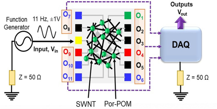
On of the most complex colloidal neuromorphic devices has been reported recently by Tanaka et al. [83] The device is fabricated from single‐walled carbon nanotubes modified with a complex modifier composed of protonated tetraphenyl porphyrin and Keggin‐type polyoxometalate, namely the [H4TPP]2[SV2W10O40] (Por‐POM) supra‐molecular assembly. This modifier has been reported to exhibit negative differential resistance and pinched hysteresis loops when deposited as thin layer on platinum comb electrodes. [84] Modified nanotubes are deposited as randomly oriented and interpenetrated network onto a prepatterned glass substrate, as shown in Figure 11. Due to high flexibility of nanotubes analogous devices can be fabricated on flexible substrates as well.
Figure 11.
The full circuit schematic of the outputs obtained from different electrode pads when a sine wave of 11 Hz, ±1 V is applied at the yellow‐coloured electrode pad connected to the SWNT (black line)/Por–POM film (green circle). A function generator is used where the output from one pole is fed as the input signal, whereas the other pole is grounded via a 50 Ω resistor (z value, orange box). All outputs are then taken from the DAQ system which is grounded via a similar 50 Ω resistor, to complete the full circuitry. Reproduced with permission. [83] Copyright 2022, John Wiley & Sons.
Application of a simple sine wave to one randomly selected input resulted in generation of a series of complex outputs at remaining device's terminals (cf. Figure 11). This behaviour results from the combination of the NDR character of the Por‐POM modifier and a complex, percolated networks of SWCNTs. Thus, a device transforming a single into into a set of time series of the character, which is a signature of brain‐like computation at the edge of chaos. This power‐law signature indicates that the signal generated from the input is solely an intrinsic property of the material. It also indicates the scale‐free nature of electrical processes in the network. Thus, the device potential can be considered as a reservoir computing system.
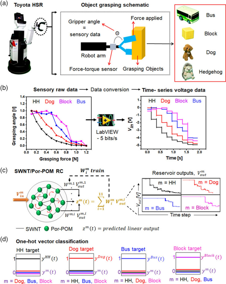
In order to verify this hypothesis tho sets of tests have been performed. The device has been used to generate any arbitrarily chosen waveform by computing linear combinations of signal from different outputs. This, however has been achieved with a significant software support ‐ the weights for these operation has been computed by ANN, which can be considered as a digital output layer of the reservoir. Finally, the device, also equipped with a simple trainable ANN output layer, has been applied for processing of signals generated by touch sensor mounted on a robotic arm (Figure 12). The gripper arm of the Toyota HSR robot has been used for gripping a series of object of different shape and softness: a toy bus model, a plastic block, a teddy dog and a plush hedgehog (Figure 12a). Recorded signals (grasping angle vs grasping force) has been translated into time‐dependent voltage signals (Figure 12b) and applied to a SWCNT/Por‐POM reservoir system, equipped with a trained ANN perceptron (Figure 12c). As a result, as series of one‐hot vector has been obtained (Figure 12d), representing very high accuracy of object recognition.
Figure 12.
Step wise object binary classification with SWNT/Por–POM reservoir: (a) The HSR (left) with a schematic of the arm (middle) connected to the gripper via force‐torque sensor gathers tactile data from the change in the gripper angle and grasping force applied to objects (right) like bus, block, dog, and hedgehog (HH) toys presented in a red box. (b) The raw sensory data (left) obtained from each of the objects are converted to time‐series voltage data using LabVIEW by sampling at 5 bits/s (left) in the range [0, −5] V as depicted graphically to the right. (c) Time series inputs from different objects m (HH, dog, bus, and block) are separately inputted into the SWNT (black line) Por–POM (green circles) reservoir with recurrent connections (red arrow), left figure. Voltage readouts from a total of i output pads each of m objects are collected as shown in the right for one of the electrode pads. (d) One‐hot vector encoding is used for binary classification. Each square box with the lines inside represents the target signal, for each of HH, dog, bus, and block. The file output is the one‐hot vector as the object to be truly predicted is true given a vector value 1 while the others a vector value 0. Reproduced with permission. [83] Copyright 2022, John Wiley & Sons.
4. Neuromorphic Gel Systems
Biological materials allow learning in response to past experiences. Classical conditioning is an elementary form of associative learning, which inspires us to explore simplified routes even for inanimate materials to respond to new, initially neutral stimuli. Neuromorphic devices implemented in gel systems are summarised in Table 3, below we discuss key prototypes.
Table 3.
Summary and comparison of reported synaptic neuromorphic gel devices.
|
Neuromorphic liquid device |
Device materials |
Availability of stimuli |
STP/STD |
LTP/LTD |
Functionality of plasticity |
Refs. |
|---|---|---|---|---|---|---|
|
Actuators |
Hydrogel/Au NPs |
light/ heat |
No |
No |
No |
[85] |
|
Transistor |
P3HT |
Electricity |
yes |
No |
yes |
[86] |
|
Transistor |
VO2 |
Electricity |
yes |
yes |
yes |
[87] |
|
Transistor |
PS‐PMMA‐PS |
Electricity |
yes |
yes |
yes |
[88] |
|
Transistor |
In−Zn‐O |
Electricity |
No |
No |
No |
[89] |
Hao Zeng and colleagues, [85] have demonstrated that soft actuators made of thermoresponsive liquid crystal networks can ‘learn’ to respond to light based on a conditioning process in which light is associated with heating. A soft microrobot based on this concept was demonstrated, including a locomotive which ‘learns to walk’ under periodic stimulation, as well as gripping devices capable of ‘recognize’ the colour of irradiation. This team predicted that actuators that algorithmically mimic basic aspects of associative learning and whose sensitivity to new stimuli can be conditioned based on previous experiences could pave the way for adaptive, autonomous soft microrobotics. [85]
Another step towards imitating psychological behaviours in synthetic materials could be to imitate the process of forgetting. Potential approaches could include the use of molecules or particles with dynamic properties, responsive material‐based logic gates, or more sophisticated intelligent responses. They showed that artificial memory could be manipulated externally using chemicals. [85]
The concept of soft robotics was demonstrated by developing a walker and colour‐recognising grippers that evolved to respond to light as a result of the association process. Meanwhile, an artificial Pavlov's dog was constructed to show off the modularity of the concept. This method allowed the construction of an artificial Pavlov's dog that could mimic a simple learning process and modify its behaviour based on its previous experience. The dynamic response of the actuators combined with the diversity of the ways in which they respond to stimuli could provide unexpected pathways toward self‐adapting, intelligent soft micro‐robots. [85]
Chuan Qian and colleagues [86] demonstrated an artificial synapse simulation based on ion‐gel gated organic field‐effect transistors (FETs) with poly(3‐hexylthiophene) (P3HT) active channels. Also, key synaptic behaviours including paired‐pulse facilitation (PPF), short‐term plasticity (STP), self‐tuning, the spike logic operation, spatiotemporal dentritic integration, and modulation were successfully mimicked.
In this work, Artificial synapses were constructed using lateral gated ion‐gel OFETs. The model simulated some key traits of synaptic behaviour, including excitatory postsynaptic currents (EPSC) and self‐tuning. Spike logic, spatiotemporal dentritic integration, and EPSC regulation were also realised with two presynaptic inputs. According to the results of XPS and in situ absorption spectra, electrical measurements revealed a direct correlation between the change of current and the [TFSA]− transferred at the interface. The intensity of π–π * absorption was found to be proportional to the amount of [TFSA]− penetrated into P3HT film. [86]
The electrolyte ion interface doping processes between the active P3HT layer and ion gels were thoroughly investigated in order to confirm the operational processes behind the fluctuations in conductivity and excitatory postsynaptic current (EPSC) in organic synaptic devices. This research was a significant step forward in the development of future artificial neuromorphic systems using newly developed ion gel gated organic synaptic devices. [86]
To imitate the functions of the biological synapse, Xing Deng's group [87] created a transparent, flexible ionic gel‐gated VO2 Mott synaptic transistor. The volatile electrostatic carrier accumulation and nonvolatile proton‐doping modulation were used to achieve short‐term and long‐term plasticity of the synapse, respectively. The channel semiconductor and gate insulator were made of epitaxial VO2 film and a rubbery solid ionic gel, respectively.
The Mott synaptic transistor was well‐suited to simulating a key sensory nerve nociceptor with threshold, relaxation, and sensitization properties. More notably, this synaptic transistor demonstrated outstanding bending stability and endurance. Under the inter‐conversion of flat and bending states, the cycle‐to‐cycle (C2 C) variance of continuous LTP and LTD measurement was as low as 3.8 %, which is analogous to the synaptic device on rigid substrate. Simulations with an artificial neural network made from these Mott transistors demonstrated that the recognition accuracy of handwritten digits can reach 95 % based on the low variance of multi‐conductance states in potentiation and depression features. [87]
Instead of modifying the pattern of presynaptic spikes, Dae‐Gyo Seo and colleagues [88] modified the synaptic decay constant of organic synaptic transistors using stable materials and device topology, allowing for a wide range of applications ranging from neuromorphic computing to neuro‐prosthetic. Figure 13 depicts a schematic of their device. The crystallinity of the polymer controlled the electrochemical doping kinetics and synaptic behaviour of artificial synaptic transistors. In this way, they demonstrated both memory and learning's long‐term retention for IGOST (ion‐gel gated organic synaptic transistors), which are useful for neuromorphic computing, as well as short‐term retention for fast synaptic transmission needed to simulate peripheral nerves such as nerves of the sensory and motor systems. Their approach combines a composite IGOST of a polymer semiconductor with an acoustic sensor coupled with a triboelectric sensor to demonstrate the feasibility of their approach in two ways. First, they simulate pattern recognition on the MNIST data‐set of handwritten digits using an IGOST with long‐term retention due to increased crystallinity. Then, they develop artificial auditory sensory nerves that combine an IGOST with short‐term retention due to disordered chain morphology in a polymer semiconductor. [88]
Figure 13.
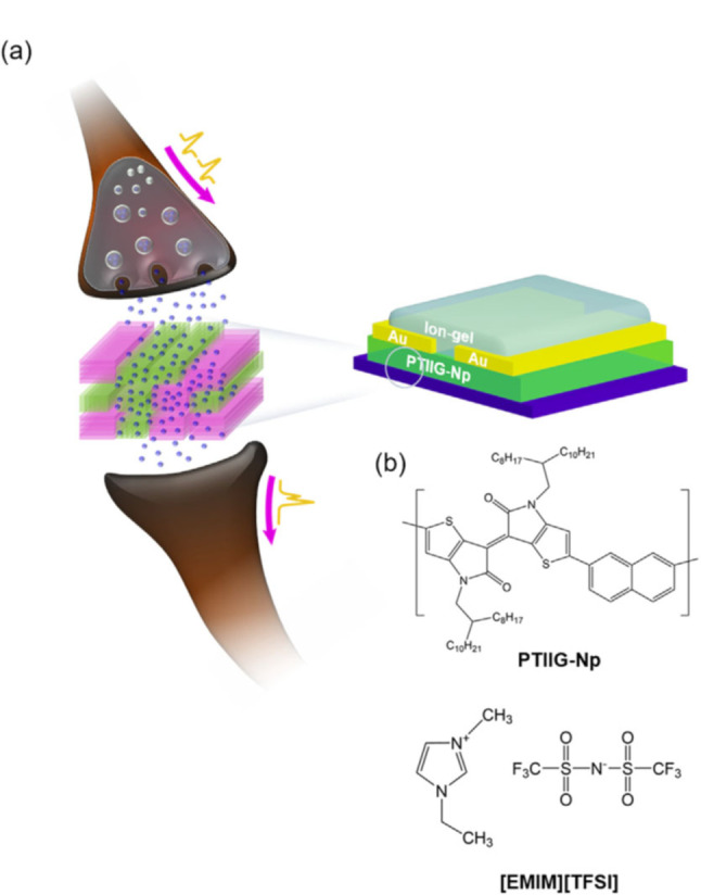
(a) Schematics of biological synapse and structure of synaptic transistor. (b) Chemical structure of poly(thienoisoindigo‐naphthalene) PTIIG−Np and 1‐ethyl‐3‐methylimidazolium bis(trifluoromethylsulfonyl)imide ([EMIM][TFSI]). Alkyl side chain (R) is 2‐octyldodecayl. Reproduced with permission. [88] Copyright 2019, Elsevier.
This team adjusted the morphology of the polymer film in order to create a variety of synaptic decay times in a single IGOST without changing the device's shape or the organic polymer composition. As the polymer crystallinity varied, the synaptic decay features changed from STP dominant to LTP dominant. Modifying the crystallinity of the synaptic decay time constant in IGOST also revealed a relationship between synaptic and morphological features. MNIST recognition accuracy for devices that used Tanh=310 °C films was 94.49 % for 8×8 MNIST data and 91.29 % for 28×28 MNIST data with LTP‐dominant synaptic decay, but these devices cannot be used for artificial sensory neural systems. On the other hand, devices that utilised Tanh=80 °C‐prepared films, demonstrated appropriate features for an artificial sensory nervous system, with STP‐dominant synaptic degeneration. Simulations and sensor integration by IGOST demonstrated the importance of engineering the microstructure of the polymer film for specific neuromorphic applications (like simulating the central or peripheral nervous system). This is the first study to demonstrate that the decay‐time constant of devices may be altered by changing the morphology of thin films, rather than changing presynaptic spike forms. In a single device, synaptic functions such as SNDP, PPF, SFDP, SVDP, and SDDP were replicated. The aim of this paper was to develop a new method for engineering organic synaptic transistors with a few necessary characteristics for use in neuromorphic computing, neural prosthetics, bio‐interface devices, and soft robotics. [88]
Ling‐an Kong and colleagues [89] created ion‐gel coupled synaptic transistors with solution‐possessed amorphous Indium‐Zinc‐Oxide (In‐Zn−O) thin films in a study. Because of the substantial electric‐double‐layer (EDL) capacitance (4.87 mF/cm2), the ion‐gel dielectric produced a strong ionic/electronic coupling on solution‐processed In‐Zn−O thin films. Synaptic functions were simulated using ion‐gel gated In‐Zn−O FETs. The presynaptic input terminal was the in‐plane gate, while the postsynaptic output terminal was the In‐Zn−O channel with source/drain electrodes. Neuro transmitters were thought to be mobile ions in ion‐gel. On the in‐plane electrodes, gate pluses were applied, which were equivalent to presynaptic spikes on the presynaptic membrane. The excitatory postsynaptic current (EPSC), spike time‐dependent EPSC, paired‐pulse facilitation (PPF), and dynamic synaptic behaviours were all replicated. [89]
The high‐mobility and low‐voltage solution‐processed In‐Zn−O FETs benefited from highly efficient ion‐gel gating. The ion‐gel gated In‐Zn−O FETs were most critically employed to simulate synaptic functions in a biological system. Using solution‐processed amorphous semiconductors, the results presented here provided a new possibility and technique for fabricating artificial synaptic circuits and neuromorphic systems. [89]
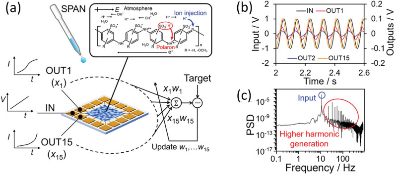
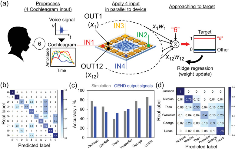
A beautiful example of reservoir computing device based on conducting polymer gel; sulfonated polyaniline (SPANI) has been reported by Tanaka, van der Wiel and Matsumoto. [90] In this system, a metal‐patterned glass substrates are covered by sulfonated polyaniline gel and kept in humid environment to prevent drying (Figure 14). The device, subjected to AC stimulation exhibited un‐pinched hysteresis loop, characteristic for redox processes in polyaniline. Furthermore, the resulting signal were rich in higher harmonics (within 10 Hz–1 kHz), indicating intrinsic power‐law dynamics (Figure 14b–c). These two features indicate the applicability of the device in neuromorphic computing: in has rich internal dynamics and memory. These features have been exploited in speech analysis, namely speaker identification. Recorded voices of six speakers (labelled as Jackson, Nicolas, Theo, Yweweler, George and Lucas) were transformed into cochleagrams, which were subsequently used as a spatiotemporal input (i. e. cochleagrams corresponding to different spoken digits were applied to different input ports of the device (Figure 15).
Figure 14.
(a) Schematic of material learning based on SPANI reservoir. There are two kinds of charge carriers in SPANI: polarons and protons. Polarons are intrinsic electrical carriers that are generated by self‐doping from sulfonic groups (red arrow). Protons can be directly injected into the SPANI molecular chain under humid conditions (blue arrow), which generates ionic conduction. Therefore, the electrical properties of SPAN can be controlled by adjusting the humidity of the environment. Various output responses including electrochemical dynamics have been used for solving complex tasks applying the reservoir computing (RC) approach. In RC, a randomly connected network (the “reservoir”) is used to create nonlinear projections of inputs into high‐dimensional space. Here, the SPANI device functions as a reservoir. The network can be trained by a simple supervised readout layer to learn linear combinations (Σ) of network states. Only the output layer weights are trained, and the random network itself remains the same during the process. (b) V–t curves of an 11 Hz sinusoidal input signal with a peak‐to‐peak voltage (VPP) of 2.0 V and nonlinear outputs for a SPANI device. The output currents are terminated with a resistance of 305 kΩ. (c) Log–log plot showing the fast Fourier transform (FFT) spectrum of output 1 (OUT1). PSD denotes power spectral density. FFT was performed for the same time periods as the Lissajous curves in Figure S5 (Supporting Information). Higher harmonic generation from a single input frequency (11 Hz) indicates that the device exhibits high‐dimensional mapping, which is essential for achieving multiple classifications with high accuracy. Reproduced with permission. [90] Copyright 2021, John Wiley & Sons.
Figure 15.
(a) Schematic of spoken‐digit classification. The spoken‐digit time series signals in the data‐set were converted to cochleagrams by separating the intensities in four frequency regions up to 130 Hz with Lyon's auditory model filtering. The cochleagrams were normalized and applied to the high‐SPAN‐concentration OEND as time series bias voltages. After recording and labelling the output from the device, the labelled outputs were classified by a ridge regression to one‐hot target vector with training (90 %) and prediction (10 %). The detail is shown in Section S8 (Supporting Information). (b) Normalized confusion matrix of spoken‐digit classification with the FSDD data‐set of one speaker (Jackson) when using OEND output signals (accuracy: 66 %). The accuracy of the echo state network (ESN) in the simulation was 78 %. (c) Comparison of the accuracy of spoken‐digit classification between the software ESN and OEND output signals for each speaker. d) Normalized confusion matrix of human classification for all speakers using OEND output signals (accuracy: 60 %). The accuracy of the ESN in the simulation was 63 %. Reproduced with permission. [90] Copyright 2021, John Wiley & Sons.
The examples presented above demonstrate the applicability of gel materials in neuromorphic computing, not only mimicking basin neural/synaptic functionalities, but also in more complex computational approaches, like reservoir computing. These computing systems are capable of complex computational tasks, like speaker identification or image recognition.
Polyaniline combined with polyethylene oxide seems to be the most successful material combination for fabrication of soft neuromimetic devices: artificial synapses and electrochemical spiking neurons. Numerous devices and complex neuromorphic circuits, along with their models and detailed application schemes has been developed over last 15 years by Victor Erokhin. His great contribution to gel neuromorphic devices, the operation of which is based by dynamic doping of conducting polymer structures accompanied by ionic diffusion has been summarised in his recent book “Fundamentals of Organic Neuromorphic Systems”. [91]
5. Conclusion
The goal of brain‐inspired neuromorphic computing is to offer an effective replica of the human brain's functionality through the use of electrical components. We overviewed the properties and materials of liquid, colloidal and gel neuromorphic systems, compared them and discussed various liquid based synaptic devices as well as their neuromorphic applications. To simulate synaptic functions, these gadgets use an aqueous solution. These liquid‐based artificial synapses have potential applications in biocompatible devices and constitute a new paradigm to explore innovative computational protocols at the liquid state. Comparative characteristics of the devices reviewed are summarised in Table 3. We find that neuromorphic device [47] and Analog : 2D‐SnO2 memtransistor [71] are devices with shortest cycles. Memory: 2D‐SnO2 memtransistor and Analog : 2D‐SnO2 memtransistor [71] are devices whose pre‐processing time is comparable with their cycle lengths. Actuator, [85] 2D‐SnO2 memtransistor and Analog:2D‐SnO2 memtransistor [71] have longest life time. Transistor, [87] 2D‐SnO2 memtransistor and Analog:2D‐SnO2 memtransistor [71] can survive largest number of cycles.
Table 4.
Comparative analysis of neuromorphic devices.
|
Device |
Cycle, ms |
Pre‐processing |
Density, device /mm2 |
Voltage range, V |
Current range |
Power consumption |
Life time |
Re‐usability, cycles |
Self‐Healing |
Refs. |
|---|---|---|---|---|---|---|---|---|---|---|
|
MoO3 device |
N/A |
N/A |
N/A |
−60 to 60 |
0.1 nA to 10 μA |
N/A |
N/A |
N/A |
No |
[70] |
|
Memory: 2D‐SnO2 memtransistor |
1000 (DC sweep) |
1 min |
N/A |
15 V to −15 V |
0.1 μA |
1.5–1.8 μW |
3 months |
1000 (DC sweep) |
N/A |
[71] |
|
Analog : 2D‐SnO2 memtransistor |
|
1 min |
N/A |
15 V to −15 V |
60–85 nA |
1.9 pJ |
3 months |
|
N/A |
[71] |
|
Transistor |
N/A |
N/A |
N/A |
−4 to 4 |
0.4 to 53 μA |
0 |
N/A |
N/A |
No |
[72] |
|
Memristor |
N/A |
N/A |
N/A |
−1.5 to 1.5 |
−100 to 140 |
150 μW |
20000 s |
100 |
No |
[75] |
|
neuromorphic device |
5 |
N/A |
0.44 cm−2 |
−8 to 5 |
0 to 0.1 mA |
69.6 nJ/event |
600 s |
200 |
No |
[47] |
|
Memristor |
N/A |
N/A |
N/A |
−3 to 3 |
−0.1 to 0.1 A |
N/A |
N/A |
N/A |
No |
[13] |
|
Optoelectronic device |
200 |
N/A |
N/A |
0 to 0.8 |
11 nA |
18 |
N/A |
N/A |
No |
[78] |
|
Li‐ion transistor |
N/A |
N/A |
N/A |
1.8 to 3.5 |
|
N/A |
N/A |
|
No |
[81] |
|
Actuators |
2000 |
N/A |
1.1 g cm−3 |
N/A |
N/A |
100 mW |
|
N/A |
No |
[85] |
|
Transistor |
200 |
N/A |
N/A |
−2 to 2 |
1.1 to 13.5 μA |
0.24 μW |
N/A |
N/A |
No |
[86] |
|
Transistor |
2000 |
N/A |
150 cm−2 |
−1.5 to 1.8 |
80 to 600 nA |
0.00018 |
N/A |
500 |
No |
[87] |
|
Transistor |
557 |
N/A |
N/A |
−1 to 2 |
0 to 6.44 mA |
0.32 μW |
N/A |
N/A |
NO |
[89] |
|
Memristor AgNO3: PVDF‐HFP : IL |
100 |
NO |
N/A |
−10 to 10 |
1 μA to 1 mA |
N/A |
|
100 |
NO |
[48] |
|
Memristor AgNO3 : PEO : IL |
100 |
NO |
N/A |
−5 to 5 |
1 μA to 1 mA |
N/A |
|
500 |
NO |
[48] |
Conflict of interest
The authors declare no conflict of interest.
6.
Biographical Information
Noushin Raeisi Kheirabadi is a Research Associate working on learning and computing in colloids within the framework of the COgITOR project. She is last year PhD candidate in Nanotechnology at Department of Materials Engineering, Isfahan University of Technology (IUT), Iran. She got a Master of Science in Nanotechnology in 2016 and a bachelor in Chemical engineering. She started experimental research on learning in colloidal systems, in the framework of European Innovation Council FETOpen project COgITOR: Colloid Cybernetic Systems at the University of the West of England (UWE). Her research focuses on learning and computing in colloidal frameworks, and triboelectric nanogenerator based on two‐dimensional Nanostructures. Her research interests include Nanotechnology, Nanomaterials and Nano‐colloids, Energy harvesting, Two‐dimensional Nanostructures, Triboelectric Nanogenerators.

Biographical Information
Alessandro Chiolerio obtained his PhD from the Physics Department of Politecnico di Torino in 2009 where he exploited quantum confinement in metals to perform information processing via the electron spin channel. In the following years, he studied transport properties of nanocomposite materials, exploring the conditions for percolation and the occurrence of resistive switching. He visited several institutes, such as NASA's Jet Propulsion Laboratory (Pasadena, USA), the Max Planck Institute (Halle, DE) and the University of the West of England (Bristol, UK) where he is visiting professor, developing ideas and performing experiments on liquid state cybernetic systems, in particular holonomic information processing. He is now at the Bioinspired Soft Robotics group of Istituto Italiano di Tecnologia, Genova (Italy). Author of more than 125 scientific articles and 32 patents, he has raised over € 10 million in competitive funding and private capital.

Biographical Information
Konrad Szaciłowski graduated from the Faculty of Chemistry, Jagiellonian University (Kraków, Poland) in 1995 (MSc) and 2000 (PhD). After habilitation (2008) he has moved from Jagiellonian University to AGH University of Science and Technology. Now he is a group leader at the Academic Center of Materials and Nanotechnology. His initial interest in photochemistry and spectroscopy of coordination compounds has gradually evolved towards molecular and nanoscale logic devices and finally towards unconventional computing. At the moment his main research interests encompass the design of inorganic materials for memristive applications, mimicking of neutral and synaptic processes in inanimate systems, and relations of musical harmony with other fields of science. Following an old Latin sentence “Repetitio est mater studiorum” he focuses on single node echo state machines with delayed feedback and reservoir computing systems. He is an author of the book “Infochemistry: Information processing at nanoscale” (Wiley 2012) and numerous papers in fields of coordination chemistry, material science, spectroscopy, catalysis, and electrochemistry. In his free time he enjoys classical music, philately and single malts from Islay and Speyside.

Biographical Information
Andrew Adamatzky is Professor of Unconventional Computing and Director of the Unconventional Computing Laboratory, Department of Computer Science, University of the West of England, Bristol, UK. He does research in molecular computing, reaction‐diffusion computing, collision‐based computing, cellular automata, slime mould computing, massive parallel computation, applied mathematics, complexity, nature‐inspired optimisation, collective intelligence and robotics, bionics, computational psychology, non‐linear science, novel hardware, and future and emergent computation. He has authored seven books, mostly notable are ‘Reaction‐Diffusion Computing’, ‘Dynamics of Crow Minds’, and ‘Physarum Machines’, and has edited 22 books in computing, most notable are ‘Collision Based Computing’, ‘Game of Life Cellular Automata’, and ‘Memristor Networks’. He has also produced a series of influential artworks published in the atlas ‘Silence of Slime Mould’. He is Founding Editor‐in‐Chief of ‘J of Cellular Automata’ and ‘J of Unconventional Computing’ and Editor‐in‐Chief of ‘J Parallel, Emergent, Distributed Systems’ and ‘Parallel Processing Letters’.

Acknowledgments
This project has received funding from the European Union's Horizon 2020 research and innovation programme FET OPEN “Challenging current thinking” under grant agreement No. 964388.
Kheirabadi N. R., Chiolerio A., Szaciłowski K., Adamatzky A., ChemPhysChem 2023, 24, e202200390.
Data Availability Statement
The data that support the findings of this study are available from the corresponding author upon reasonable request.
References
- 1. Chiolerio A., Adv. Intell. Syst. 2020, 1. [Google Scholar]
- 2.A. Adamatzky (Editor), Advances in unconventional computing, Springer 2016.
- 3.A. Adamatzky, Handbook of Unconventional Computing, World Scientific 2021.
- 4. Mead C., Proc. IEEE 1990, 78, 1629. [Google Scholar]
- 5. Gorecki J., Gorecka J. N., Int. J. Unconv. Comput. 2006, 2. [Google Scholar]
- 6. Szymanski J., Gorecka J. N., Igarashi Y., Gizynski K., Gorecki J., Zauner K.-P., Planque M., et al., Int. J. Unconv. Comput. 2011, 7, 185. [Google Scholar]
- 7.J. Stovold, S. O'Keefe, in International Conference on Information Pro- cessing in Cells and Tissues, Springer 2012.
- 8.J. Gorecki, J. Gorecka, Y. Igarashi, K. Yoshikawa, in Nature Computing, Springer 2009.
- 9. Gentili P. L., Horvath V., Vanag V. K., Epstein I. R., Int. J. Unconv. Comput. 2012, 8, 177. [Google Scholar]
- 10. Vanag V. K., Chaos 2019, 29, 083104. [DOI] [PubMed] [Google Scholar]
- 11. Gorecki J., Gorecka J. N., Adamatzky A., Phys. Rev. E 2014, 89, 042910. [DOI] [PubMed] [Google Scholar]
- 12. Gruenert G., Gizynski K., Escuela G., Ibrahim B., Gorecki J., Dittrich P., Int. J. Neural Syst. 2015, 25, 1450032. [DOI] [PubMed] [Google Scholar]
- 13. Mayne R., Draper T. C., Phillips N., Whiting J. G., Weerasekera R., Fullarton C., de Lacy Costello B. P., Adamatzky A., Langmuir 2019, 35, 13182. [DOI] [PMC free article] [PubMed] [Google Scholar]
- 14. Indiveri G., Horiuchi T. K., Front. Neurol. Neurosci. 2011, 5, 118. [DOI] [PMC free article] [PubMed] [Google Scholar]
- 15. Chicca E., Stefanini F., Bartolozzi C., Indiveri G., Proc. IEEE 2014, 102, 1367. [Google Scholar]
- 16. Pecqueur S., Vuillaume D., Alibart F., J. Appl. Phys. 2018, 124, 151902. [Google Scholar]
- 17. Chiolerio A., Chiappalone M., Ariano P., Bocchini S., Front. Neurol. Neurosci. 2017, 11. [DOI] [PMC free article] [PubMed] [Google Scholar]
- 18. Chicca E., Indiveri G., Appl. Phys. Lett. 2020, 116, 120501. [Google Scholar]
- 19. LeCun Y., Bengio Y., Hinton G., Nature 2015, 521, 436. [DOI] [PubMed] [Google Scholar]
- 20. Sangwan V. K., Hersam M. C., Nat. Nanotechnol. 2020, 15, 517. [DOI] [PubMed] [Google Scholar]
- 21. McCulloch W. S., Pitts W., Bull. Math. Biol. 1943, 5, 115. [Google Scholar]
- 22. Rosenblatt F., Psychol. Rev. 1958, 65, 386. [DOI] [PubMed] [Google Scholar]
- 23.M. Bear, B. Connors, M. Paradiso, in Neuroscience: Exploring the Brain, Philadelphia: Wolters Kluwer Health 2015.
- 24. Hodgkin A. L., Huxley A. F., Physiol. J. 1952, 117, 500. [DOI] [PMC free article] [PubMed] [Google Scholar]
- 25.L. Chua, in Handbook of Memristor Networks, Springer 2019.
- 26. Pershin Y. V., Di Ventra M., Adv. Phys. 2011, 60, 145. [Google Scholar]
- 27. Rumelhart D. E., Hinton G. E., Williams R. J., Nature 1986, 323, 533. [Google Scholar]
- 28. Maass W., Neural Netw. 1997, 10, 1659. [Google Scholar]
- 29. Christensen D. V., Dittmann R., Linares-Barranco B., Sebastian A., Le Gallo M., Redaelli A., Slesazeck S., Mikolajick T., Spiga S., Neuromorphic Comput. Eng. 2022, 2, 022501. [Google Scholar]
- 30. James C. D., Aimone J. B., Miner N. E., Vineyard C. M., Rothganger F. H., Carlson K. D., Mulder S. A., Draelos T. J., Faust A., Biol. Inspired Cogn. Archit. 2017, 19, 49. [Google Scholar]
- 31. Krestinskaya O., James A. P., Chua L. O., IEEE Trans. Neural Netw. Learn. Syst. 2019, 31, 4. [DOI] [PubMed] [Google Scholar]
- 32.B. Murmann, B. Hoeffliger, Nanochips 2030, Springer Nature 2020.
- 33. Tuma T., Pantazi A., Le Gallo M., Sebastian A., Eleftheriou E., Nat. Nanotechnol. 2016, 11, 693. [DOI] [PubMed] [Google Scholar]
- 34. Chua L., IEEE Trans. Circuits Syst. 1971, 18, 507. [Google Scholar]
- 35. Rajan K., Bejtka K., Bocchini S., Perrone D., Chiappone A., Roppolo I., Pirri C. F., Ricciardi C., Chiolerio A., J. Mater. Chem. C 2017, 6144–6155. [Google Scholar]
- 36. Porro S., Risplendi F., Cicero G., Bejtka K., Milano G., Rivolo P., Jasmin A., Chiolerio A., Pirri C. F., Ricciardi C., J. Mater. Chem. C 2017, 5, 10517. [Google Scholar]
- 37. Porro S., Bejtka K., Jasmin A., Fontana M., Milano G., Chiolerio A., Pirri C. F., Ricciardi C., Nanotechnology 2018, 29, 10517. [DOI] [PubMed] [Google Scholar]
- 38. Shulaker M. M., Hills G., Park R. S., Howe R. T., Saraswat K., Wong H.-S. P., Mitra S., Nature 2017, 547, 74. [DOI] [PubMed] [Google Scholar]
- 39.V. C. Müller 2020.
- 40. Lee Y., Lee T.-W., Acc. Chem. Res. 2019, 52, 964. [DOI] [PubMed] [Google Scholar]
- 41. Goldmann M., Köster F., Lüdge K., Yanchuk S., Chaos 2020, 30, 093124. [DOI] [PubMed] [Google Scholar]
- 42. Chen T., Bobbert P., van der Wiel W., Small Science 2021, 1, 2000014. [Google Scholar]
- 43. Wilczek F., Phys. Rev. Lett. 2012, 109, 160401. [DOI] [PubMed] [Google Scholar]
- 44.A. Bandyopadhay, Nanobrain CRC Press 2020.
- 45. Izhikevich E. M., Neural Comput. 2006, 18, 245. [DOI] [PubMed] [Google Scholar]
- 46. Schmid H., Avitabile D., Montbrió E., PLoS Comput. Biol. 2018, 14, e1006430. [DOI] [PMC free article] [PubMed] [Google Scholar]
- 47. Kim D., Lee J.-S., NPG Asia Mater. 2020, 12, 1. [Google Scholar]
- 48. Rajan K., Roppolo I., Chiappone A., Bocchini S., Perrone D., Pirri C. F., Ricciardi C., Chiolerio A., Appl. Surf. Sci. 2018, 443, 475. [Google Scholar]
- 49. Wlazlak E., Przyczyna D., Gutierrez R., Cuniberti G., Szacilowski K., Jpn. J. Appl. Phys. 2020, 59, SI0801. [Google Scholar]
- 50. Przyczyna D., Zawal P., Mazur T., Strzelecki M., Gentili P. L., Szacilowski K., Jpn. J. Appl. Phys. 2020, 59, 050504. [Google Scholar]
- 51. Chun H., Chung T., Annu. Rev. Anal. Chem. 2015, 8, 19.1. [DOI] [PubMed] [Google Scholar]
- 52. Pérez-Mitta G., Albesa A. G., Trautmann C., Toimil-Molaresb M. E., Azzaroni O., Chem. Sci. 2017, 8, 890. [DOI] [PMC free article] [PubMed] [Google Scholar]
- 53. Wang M., Hou Y., Yu L., Hou X., Nano Lett. 2020, 20, 6937. [DOI] [PubMed] [Google Scholar]
- 54. Hou Y., Hou X., Science 2021, 373, 628. [DOI] [PubMed] [Google Scholar]
- 55. Robin P., Kavokine N., Bocquet L., Science 2021, 373, 687. [DOI] [PubMed] [Google Scholar]
- 56. Yang J. J., Xia Q., Nat. Mater. 2017, 16, 396. [DOI] [PubMed] [Google Scholar]
- 57. Fu Y. M., Wan C. J., Zhu L. Q., Xiao H., Chen X. D., Wan Q., Adv. Biosyst. 2018, 2, 1700198. [Google Scholar]
- 58. Marx G., ACS Chem. Neurosci. 2012, 3, 633. [DOI] [PMC free article] [PubMed] [Google Scholar]
- 59. Chiolerio A., Bocchini S., Crepaldi M., Bejtka K., Pirri C. F., Synth. Met. 2017, 229, 72. [Google Scholar]
- 60. Maass W., Natschläger T., Markram H., Neural Comput. 2002, 14, 2531. [DOI] [PubMed] [Google Scholar]
- 61.A. Polepalli, N. Soures, D. Kudithipudi, in 2016 IEEE International Con- ference on Rebooting Computing (ICRC), IEEE 2016.
- 62.M. R. Smith, A. J. Hill, K. D. Carlson, C. M. Vineyard, J. Donaldson, D. R. Follett, P. L. Follett, J. H. Naegle, C. D. James, J. B. Aimone, in International Joint Conference on Neural Networks (IJCNN), IEEE 2017.
- 63. Aussillous P., Quéré D., Nature 2001, 411, 924. [DOI] [PubMed] [Google Scholar]
- 64. Draper T. C., Fullarton C., Phillips N., de Lacy Costello B. P., Adamatzky A., Sci. Rep. 2018, 8, 1. [DOI] [PMC free article] [PubMed] [Google Scholar]
- 65.T. C. Draper, C. Fullarton, N. Phillips, B. P. de Lacy Costello, A. Adamatzky, in International Conference on Unconventional Computation and Natural Computation, Springer 2018.
- 66. Draper T. C., Fullarton C., Mayne R., Phillips N., Canciani G. E., de Lacy Costello B. P., Adamatzky A., Soft Matter 2019, 15, 3541. [DOI] [PubMed] [Google Scholar]
- 67.A. Adamatzky, in Collision-Based Computing, Springer 2002.
- 68. Draper T. C., Fullarton C., Phillips N., de Lacy Costello B. P., Adamatzky A., Mater. Today 2017, 20, 561. [Google Scholar]
- 69. He Y., Jiang S., Chen C., Wan C., Shi Y., Wan Q., J. Appl. Phys. 2021, 130, 190904. [Google Scholar]
- 70. Zhang C., Pudasaini P. R., Oyedele A. D., Ievlev A. V., Xu L., Haglund A. V., Noh J. H., Wong A. T., Xiao K., Ward T. Z., ACS Appl. Mater. Interfaces 2018, 10, 22623. [DOI] [PubMed] [Google Scholar]
- 71. Huang C.-H., Chang H., Yang T.-Y., Wang Y.-C., Chueh Y.-L., Nomura K., ACS Appl. Mater. Interfaces 2021, 13, 52822. [DOI] [PubMed] [Google Scholar]
- 72. Liu Y., Zhong J., Li E., Yang H., Wang X., Lai D., Chen H., Guo T., Nano Energy 2019, 60, 377. [Google Scholar]
- 73. Wang T.-Y., He Z.-Y., Chen L., Zhu H., Sun Q.-Q., Ding S.-J., Zhou P., Zhang D. W., Micromachines 2018, 9, 239. [DOI] [PMC free article] [PubMed] [Google Scholar]
- 74. Cucchi M., Kleemann H., Tseng H., Ciccone G., Lee A., Pohl D., Leo K., Adv. Electron. Mater. 2021, 7, 2100586. [Google Scholar]
- 75. Khan M. U., Saqib Q. M., Chougale M. Y., Shaukat R. A., Kim J., Bae J., Microsyst. Nanoeng. 2021, 7, 1. [DOI] [PMC free article] [PubMed] [Google Scholar]
- 76. Rajan K., Bocchini S., Chiappone A., Roppolo I., Perrone D., Castellino K., Bejtka >M., Lorusso M., Ricciardi C., Pirri C. F., Chiolerio A., Flex. Print. Electrons 2017, 2. [Google Scholar]
- 77. Rajan K., Garofalo E., Chiolerio A., Sensors 2018, 18. [DOI] [PMC free article] [PubMed] [Google Scholar]
- 78. Tan H., Ni Z., Peng W., Du S., Liu X., Zhao S., Li W., Ye Z., Xu M., Xu Y., et al., Nano Energy 2018, 52, 422. [Google Scholar]
- 79. Pilarczyk K., Podborska A., Lis M., Kawa M., Migda D., Szacilowski K., Adv. Electron. Mater. 2016, 2, 1500471. [Google Scholar]
- 80. Przyczyna D., Lis M., Pilarczyk K., Szacilowski K., Molecules 2019, 24, 2738. [DOI] [PMC free article] [PubMed] [Google Scholar]
- 81. Yu H., Holtz M. E., Gong Y., Pearson J., Ren Y., Herzing A. A., Zhang X., Takeuchi I., Phys. Rev. Mater. 2021, 5, 115401. [Google Scholar]
- 82. Chiolerio A., Roppolo I., Bejtka K., Asvarov A., Pirri C. F., RSC Advances 2016, 6, 56661. [Google Scholar]
- 83. Banerjee D., Kotooka T., Azhari S., Usami Y., Ogawa T., Gimzewski J. K., Hirofumi Tanaka H. T., Adv. Intell. Syst. 2022, 2100145. [Google Scholar]
- 84. Yamazaki Y., Ichi Yamashita K., Tani Y., Aoyama T., Ogawa T., J. Mater. Chem. C 2020, 8, 14423. [Google Scholar]
- 85. Zeng H., Zhang H., Ikkala O., Priimagi A., Matter 2020, 2, 194. [DOI] [PMC free article] [PubMed] [Google Scholar]
- 86. Qian C., Sun J., Kong L.-a., Gou G., Yang J., He J., Gao Y., Wan Q., ACS Appl. Mater. Interfaces 2016, 8, 26169. [DOI] [PubMed] [Google Scholar]
- 87. Deng X., Wang S.-Q., Liu Y.-X., Zhong N., He Y.-H., Peng H., Xiang P.-H., Duan C.-G., Adv. Funct. Mater. 2021, 2101099. [Google Scholar]
- 88. Seo D.-G., Lee Y., Go G.-T., Pei M., Jung S., Jeong Y. H., Lee W., Park H.-L., Kim S.-W., Yang H., et al., Nano Energy 2019, 65, 104035. [Google Scholar]
- 89. Kong L.-a., Sun J., Qian C., Gou G., He Y., Yang J., Gao Y., Org. Electron. 2016, 39, 64. [Google Scholar]
- 90. Usami Y., van de Ven B., Mathew D. G., Chen T., Kotooka T., Kawashima Y., Tanaka Y., Otsuka Y., Ohoyama H., Tamukoh H., Tanaka H., van der Wiel W. G., Matsumoto T., Adv. Mater. 2021, 33, 2102688. [DOI] [PMC free article] [PubMed] [Google Scholar]
- 91.V. Erokhin, Fundamentals of Organic Neuromorphic Systems, Springer Nature 2022.
Associated Data
This section collects any data citations, data availability statements, or supplementary materials included in this article.
Data Availability Statement
The data that support the findings of this study are available from the corresponding author upon reasonable request.


