Abstract
Understanding the mechanisms that connect heat and electron transport with crystal structures and defect chemistry is fundamental to develop materials with thermoelectric properties. In this work, we synthesized a series of self‐doped compounds Cu2+x Mn1−x GeS4 through Cu for Mn substitution. Using a combination of powder X‐ray diffraction, high resolution transmission electron microscopy and precession‐assisted electron diffraction tomography, we evidence that the materials are composed of interconnected enargite‐ and stannite‐type structures, via the formation of nanodomains with a high density of coherent interfaces. By combining experiments with ab initio electron and phonon calculations, we discuss the structure–thermoelectric properties relationships and clarify the interesting crystal chemistry in this system. We demonstrate that excess Cu+ substituted for Mn2+ dopes holes into the top of the valence band, leading to a remarkable enhancement of the power factor and figure of merit ZT.
Keywords: Inorganic Chemistry, Solid-State Structures, Stannite, Sulfides, Thermoelectric, Wurtzite
A particular biphasic compound, which consists of interconnected enargite‐ and stannite‐type tetrahedral frameworks at the nanoscale, has been synthesized. The complex crystal chemistry of such nanocomposites raises the issue of the role of the two structures and of their interfaces in the mechanism governing their electrical and thermal conductivities.
Introduction
Copper rich sulfides represent a remarkable source of thermoelectric materials for energy recovery from waste heat due to their abundance as minerals, non‐toxicity and low cost in view of industrial application. Numerous studies have been focused on the thermoelectric performances of these materials, whose material conversion efficiency characterized by the figure of merit ZT=S 2 T/ρκ (S, ρ, κ, and T represent the Seebeck coefficient or thermopower, electrical resistivity, thermal conductivity, and operating temperature, respectively) seems to have reached the ceiling of about 1 at 700 K. [1] It is now well established that the transport properties of these materials originate from the CuI‐CuII mixed valence [2] allowing p‐type carrier delocalization over the Cu−S network. In contrast, the role of the structure and chemical bond on the thermoelectric properties of these materials is so far not really understood. A recent review of copper sulfides [3] shows that the thermoelectric properties of these systems are mainly observed for the sphalerite derivatives, while very little is known about the possible synthesis of thermoelectric wurtzite derivatives, in spite of the fact that, in both structural families, univalent copper exhibits the tetrahedral coordination and they differ only in the packing of such tetrahedra: fcc and hcp for sphalerite and wurtzite, respectively.
This is illustrated by the sulfides with generic formula Cu2 MSnS4 (with M=Mn, Fe, Co, Zn, Cd, Hg) and Cu2 MGeS4 (with M=Fe, Co, Hg) whose tetragonal structure (Figure 1a) is based on the sphalerite (zinc blende) sublattice,[ 4 , 5 , 6 , 7 , 8 ] and have been studied for their attractive thermoelectric performances,[ 9 , 10 , 11 , 12 , 13 , 14 , 15 , 16 , 17 , 18 , 19 , 20 ] while no evidence of high thermoelectric performances has been pointed out for the Cu2 MGeS4 sulfides with M=Mn, Ni, Zn, Cd, whose orthorhombic enargite structure (Figure 1b) is derived from the wurtzite.[ 4 , 5 , 6 , 7 , 8 , 21 ] Nevertheless, recent investigations by Tanimoto et al. [22] have shown that the enargite‐type sulfide Cu3P1−x Ge x S4 exhibits attractive thermoelectric performance with a figure of merit ZT of 0.5 at 673 K. Bearing in mind that the latter compound crystallizes in an orthorhombic enargite structure derived from the wurtzite, [23] we have embarked in the investigation of the Cu2 MGeS4 wurtzite derivatives. We report herein on the self‐copper doped Cu2+x Mn1−x GeS4 sulfide which exhibits thermoelectric properties with a ZT figure of merit up to 0.35 at 700 K. We show that this material, which appears in a first step from powder X‐ray diffraction (PXRD) as biphasic, is a spontaneous composite consisting of two interconnected enargite‐ and stannite‐type structures at a nanoscale without significant compositional changes.
Figure 1.
Crystal structure representation of Cu2 MGeS4 phases with a) a tetragonal stannite‐type structure (M=Fe, Co, Hg) and b) an orthorhombic enargite‐type structure (M=Mn, Ni, Zn, Cd). Key: Cu in blue; M in red; Ge in grey; S in yellow.
Results and Discussion
Structural analysis
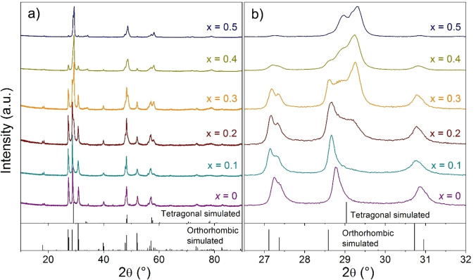
PXRD patterns of the sintered samples in the Cu2+x Mn1−x GeS4 series are displayed in Figure 2a. For pristine sample (x=0), the XRD pattern corresponds to the orthorhombic enargite‐type phase ( ), in agreement with previous studies on Cu2MnGeS4[ 4 , 6 , 7 , 8 ] and other quaternary compounds Cu2 MGeS4 (M=Ni, Zn, Cd) and Cu2 MSiS4 (M=Mn, Fe, Zn, Cd, Hg).[ 4 , 6 , 7 , 8 , 24 ] with traces of the NaCl‐type MnS phase. With increasing x, additional reflections (Figure 2b) indicate the presence of a secondary phase possibly isostructural to some stannite‐type tetragonal phases ( , i.e. Cu2 MGeS4 (M=Fe, Co, Hg) and Cu2 MSnS4 (M=Mn, Fe, Co, Zn, Cd, Hg).[ 4 , 5 , 6 , 7 , 8 ] From x=0.2, the content of the assumed tetragonal phase increases at the expense of the orthorhombic phase, the content of which significantly decreases in x=0.4 and x=0.5 samples. A similar trend has been observed in the solid solution Cu2Cd1−x Mn x GeSe4 (0≤x≤1), [25] where the tetragonal stannite‐type structure is stabilized for 0≤x<0.2, and the orthorhombic structure is formed for 0.2≤x≤1.0. Note that, in nanoparticles of Cu3Zn1−x Al x SnS5−y and Cu2Sn1−x Zn x S3, mixtures of tetragonal and orthorhombic phases were also observed depending on the sample composition and preparation.[ 26 , 27 ]
Figure 2.
a) PXRD patterns obtained for the Cu2+x Mn1−x GeS4 series. Orthorhombic and tetragonal simulated peaks intensities and positions correspond, respectively, to enargite ( ) and stannite ( ) structures. b) Enlarged area of the PXRD patterns.
Attempts to perform Rietveld refinements of the XRD patterns failed for all the samples; even for x=0, the diffraction peaks are anisotropically broadened, with strong not‐instrumental asymmetry and their intensities deviate significantly from the calculated ones using the orthorhombic phase (enargite). Such characteristics are common to all the compositions in this series, for peaks ascribed to the tetragonal and the orthorhombic phases, indicating the existence of small crystallites and/or structural defects.
To investigate further the structure and microstructure of the Cu2+x Mn1−x GeS4 series, scanning (SEM) and transmission electron microscopy (TEM) analyses were performed. TEM bright field images (Figure S1) show that the pristine Cu2MnGeS4 has fine isotropic grains (typically smaller than 100 nm) with contrasts showing stripe‐like patterns that are often related to stacking faults and/or crystal twins. To confirm the formation of enargite phase, we used precession electron diffraction tomography (PEDT), a single crystal diffraction technique suitable for analyzing the structure of sub‐micrometer size grains. Using an electron beam of about 70 nm, PEDT data (Table S1) were collected on portions of crystals as free as possible of stripe‐like contrasts. From the reciprocal space sections (Figure S2) reconstructed from the PEDT data, the reflections can be sorted in two categories: strong ones related the wurtzite subcell and weak ones indicating the existence of a superstructure to be associated with an orthorhombic enargite‐type cell. Subsequent structure refinements (Table 1), performed taking into account dynamical diffraction effects, [28] confirm this result which is supported by calculations of bond valence sums (BVS) identifying three different cationic sites compatible with Ge4+, Mn2+ and Cu+. Although this result supports enargite formation in the sample, some disorder must also be present as indicated by the presence of diffuse scattering lines along the c* direction for the rows with index h−2k=4n (see Figure S2). In Figure S3, the HRTEM images show that the stripe‐like contrast observed in bright field low magnification (Figure S1(a,b)) cannot be understood only considering the orthorhombic enargite phase. The stripe‐like patterns observed in numerous grains (Figure S3a) are actually composed of planar defects (e.g., nanotwins and stacking faults, Figures S3b and S3c) involving the coexistence of orthorhombic enargite and another phase, later confirmed as tetragonal stannite. Despite the coherent interface (Figure S3d), there are plenty of incoherent phase boundaries between these two phases which give rise to array of dislocations at the boundaries and the intersection of these two phases will lead to lattice distortions in local areas. It is suggested that the dislocations and local distortions may contribute to the origin of the structural disorder observed in Figure S2 and broad diffraction peaks observed in Figure 2, but other features cannot be completely excluded.
Table 1.
Atomic parameters obtained for the sample Cu2MnGeS4 based on the structure refinements against PEDT data (Table S1). Site occupancy are all equal to 1. The BVS column gives the bond valence sums obtained for each atomic position. Pmn21 a=7.69(1) Å, b=6.541(7) Å and c=6.340(9) Å.
|
Atom label |
x |
y |
z |
Uiso [Å2] |
BVS |
|---|---|---|---|---|---|
|
Ge1 |
0.5 |
0.8254(4) |
0.2554(10) |
0.0056(7) |
3.63(3) |
|
Mn1 |
0 |
0.8354(5) |
0.2588(12) |
0.0123(9) |
2.06(2) |
|
Cu1 |
0.2507(4) |
0.3257(3) |
0.25[a] |
0.0174(6) |
1.20(1) |
|
S1 |
0.2640(5) |
0.6617(5) |
0.3764(10) |
0.0108(7) |
2.06(2) |
|
S2 |
0 |
0.1889(7) |
0.3979(14) |
0.0022(13) |
2.01(3) |
|
S3 |
0.5 |
0.1544(8) |
0.3630(14) |
0.0115(12) |
1.97(2) |
[a] fixed parameter (polar space group)
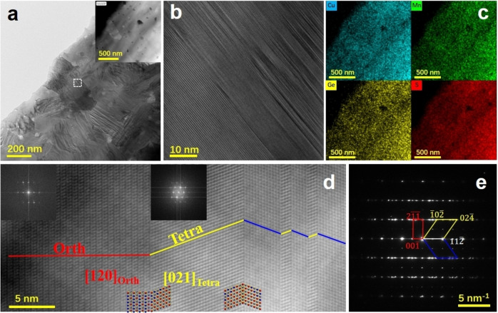
After realizing that the x=0 sample was in fact structurally quite complex, we have examined the other samples in the series. Using the sample x=0.3 as an illustration, bright field TEM images (see Figure 3) show that the grain growth becomes more significant with the increase of Cu and the decrease of Mn contents, leading to larger elongated grains (See Figure S1 for comparison and SEM results below). Interestingly, a large majority of grains exhibit stripe‐like contrasts, particularly in the elongated grains, as seen in Figure 3a. The HRTEM image of Cu2.3Mn0.7GeS4 (corresponding to the dotted region in Figure 3a) further reveals that, besides the dense stacking faults or twin boundaries, distinct crystal lattices were observed to coexist within the same crystallite from the lower left to upper right part of Figure 3b.
Figure 3.
Microstructure characterization of Cu2.3Mn0.7GeS4 sample. a,b) TEM images. c) EDX mapping of the corresponded area in the inset HAADF image of (a), HAADF image (d) and (e) the corresponding SAED pattern of Cu2.3Mn0.7GeS4.
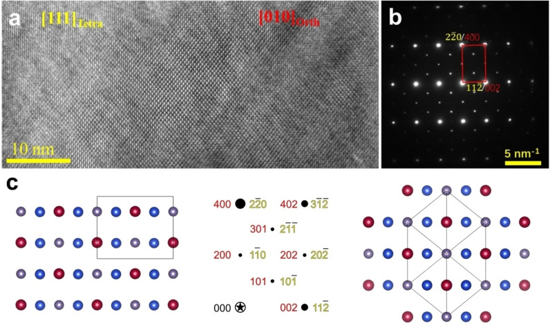
Benefitting from the incoherent imaging of HAADF‐STEM, the actual atomic columns can be deduced directly from the HAADF image. Figure 3d shows the HAADF image from the same region of Figure 3c (with scanning direction rotated), where two distinct lattices can be identified. The squared‐like crystal lattice in the left part can be assigned to an orthogonal lattice compatible with enargite structure (red line) while the right part composed of nano‐twins (even with several atomic layers thick) can be assigned to a tetragonal lattice compatible with stannite structure (yellow and blue lines). These two phases have indeed specific orientation relationships, forming coherent interfaces, that is [120]Orth//[021]Tetra and (001)Orth//(11 )Tetra. Figure 3e shows the SAED pattern corresponding to the region of Figure 3d, in which both the two distinct phases and twin structures were identified. We also proceed to a 3D reciprocal space reconstruction using PEDT data (Table S2) collected on portions of crystals. Doing so, we were able to confirm the presence of enargite‐ and stannite‐type structures (see their distinctive signature in the form of weak reflections in Figures S4 and S5, respectively). Subsequent structure refinements (Table S3), performed taking into account dynamical diffraction effects, confirm this result with, in both cases, the identification of three different cationic sites compatible with Ge4+, Mn2+ and Cu+. While the refinements allow to distinguish the cationic sites, the stoichiometry Cu2MnGeS4 was imposed considering that potential Mn2+ substitution by Cu+ would be difficult to probe. It is worth mentioning that the cationic arrangements projected along the [010]Orth and [111]Tetra are the same in both structure (see Figure 4a,b), which should account for the perfect orientation relationships by sharing coherent interfaces between these two phases. When the grain (in Figure S6) rotates ≈30° along the direction parallel to the coherent interface, the previously distinguished two phases and nanotwins disappeared and a single‐crystal‐like feature appears (see Figure 4a). While PXRD suggested a phase mixing with possibly both enargite and stannite phases, electron microscopy investigations reveal a more complex situation. If areas of several tens of nanometers can be regarded as either enargite or stannite, a significant part of the sample does exhibit a fine and coherent intermixing of these two phases even within one single grain via the formation of nano‐twins with a high density of coherent interfaces. Note that coherent interfaces and stacking faults were also reported in enargite‐luzonite minerals. [29]
Figure 4.
a) HRTEM images and b) SAED patterns of Cu2.3Mn0.7GeS4 along the direction where the projection of enargite and stannite structure lead to a coincidence lattice (highlighted in red), c) cationic positions of enargite (left) and stannite (right) as obtained from the structure refinement against PEDT data. Mn, Cu and Ge are respectively represented in red, blue and grey. In the central part of c), the coincidence lattice in reciprocal space is indexed using both lattices: red for enargite and yellow for stannite.
Stacking simulation
Based on the TEM study, it is possible to reevaluate the previously collected XRD pattern with a non‐periodic approach, i.e. using the general recursion method for crystals containing coherent planar faults developed by Treacy et al., [30] implemented in DIFFaX and successor software FAULTS [31] used in the present work. Without entering into the calculation details, in such a method, the crystal is represented as a layered structure in which the layer sequence and their stacking vector are determined by a probabilistic law.
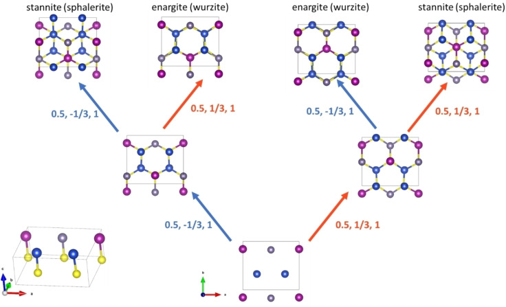
Using such approach, the enargite and stannite structures could be built as layered structure with a stacking along the c axis of the enargite cell ([11 ] for stannite) in agreement with the direction of the diffuse line in the reciprocal space reconstruction (see Figures S4 and S2). Along such direction, both structures could be represented as the stacking of diamond lattices layer of Cu2MnGeS4, using a cell derived from enargite (a layer=a enargite, b layer=b enargite and c layer= c enargite) which has the same a and b axes of enargite (see Figure 5). The component along the a and b axes of the stacking vector are determined by conserving the coincidence lattice along the enargite b axis (Figure 4) and the recommendation from DFT calculation to maintain a coherent interface. The only two stacking vectors meeting the requirements were v1=[ , , 1] and v2=[ , − , 1]. The stannite structure is formed by repeatedly using the same stacking vector while the enargite results from the alternation of one vector with the other. In such a framework, both the structure and the defaults presented in Figures 2, S3, and S6 could be represented by a change in the sequence of the vectors.
Figure 5.
Layer cell used to build the composite crystal enargite/stannite and stacking vector used during refinement.
enargite: v1, v2, v1, v2, v1,…
stannite: v1, v1, v1, v1,….. or v2, v2, v2, v2, …….
stacking fault in enargite v1, v2, v1, v1, v2, v1,… or v2, v1, v2, v2, v1, v2,…
twin boundary in stannite v1, v1, v1, v2, v2, v2,… or v2, v2, v2, v1, v1, v1,…
coherent interface stannite/enargite v2, v1, v2, v1, v1, v1, … or v2, v1, v2, v2, v2, v1, …
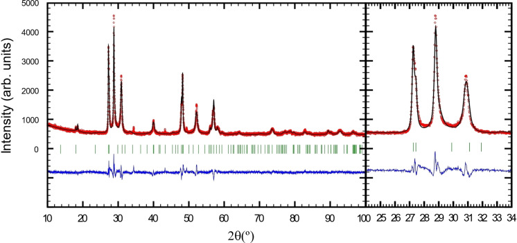
Using such an approach, it has been possible to fit the powder diffraction of Cu2MnGeS4 sample (Figure 6, results of the fit in Table S4) which results in a probability of around 4 % passing from an enargite type structure to a stannite and ≈15 % to pass from stannite to enargite and an almost negligible difference between the c axis of enargite and stannite layers (axes a and b are equal by construction). SAED simulated images using the model resulting from powder refinement for h0l and 0kl planes (Figure S4) present some discrepancies with respect to the TEM reconstructed reciprocal space for the same sample; the diffuse strikes do not corroborate the selection rule h−2k=4n. However, they are in quite good agreement with data collected on the enargite zone of sample Cu2.3Mn0.7GeS4 (Figure S4). Such observation could be explained by the fact that only the most regular region has been selected to solve the structure by TEM. However, in the powders of Cu2MnGeS4 analyzed by XRD, many more defects are present. Note that, for the samples with x >0.1, the patterns become more complicated and are impossible to fit using the model applied for x=0 (See discussions in Supporting Information).
Figure 6.
Faults fit of XRPD patterns obtained for the Cu2MnGeS4 sample
Microstructural analysis
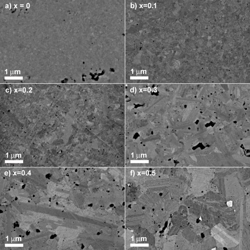
SEM images of polished surfaces (Figure 7) confirm the TEM observations. Pristine sample contains very small and isotropic grains of around 100–300 nm (Figure 7a). Only traces of CuS impurities (white contrast) are detected in x=0.5 sample (Figure 7f) which suggests the limit of solubility is reached. Such small isotropic grains are typically observed in copper‐based sulfide compounds prepared by mechanical alloying combined with spark plasma sintering at relatively low temperature (873 K or lower).[ 32 , 33 , 34 ] Interestingly, when increasing x, the grain size increases and the shape becomes more elongated. A mixture of isotropic and anisotropic grains is observed for all compositions, with a majority of elongated grains for x≥0.3 (Figure 7d–f). SEM‐EDS analysis revealed a slight difference of composition between elongated and isotropic grains (See Figure S7 for x=0.3). While Ge seems homogeneously distributed, elongated (dark grey) grains are Mn‐rich/Cu‐poor compared to the nominal Cu2.3Mn0.7GeS4 with an average composition Cu2.2Mn0.8GeS4. Isotropic (light grey) grains are Mn‐poor/Cu‐rich with an average composition Cu2.5Mn0.5GeS4. For the expanded area, STEM‐EDS shows relative homogeneous distributions (as show in Figure 3c), however, there are obvious chemical difference between dark and bright grains (see Figure S8). Although the EDS background of the TEM molybdenum (Mo) grid affects the quantitation of sulphur (S) due to the extremely close X‐ray peaks, the cationic chemical compositions of different grains/regions can be probed. An average approximative composition of “Cu2.38Mn0.87Ge0.73S4” was obtained for the whole area in Figure S8, and “Cu2.40Mn0.76Ge0.77S4”, “Cu2.65Mn0.78Ge0.82S4” and “Cu2.19Mn0.88Ge0.74S4” for two light grey and one dark grey grains. Thus, STEM‐EDS images and corresponding FFT patterns indicate that Cu‐rich lamella has tetragonal structure while Mn‐rich elongated grain possesses orthorhombic phase.
Figure 7.
SEM images of polished surfaces in the Cu2+x Mn1−x GeS4 series.
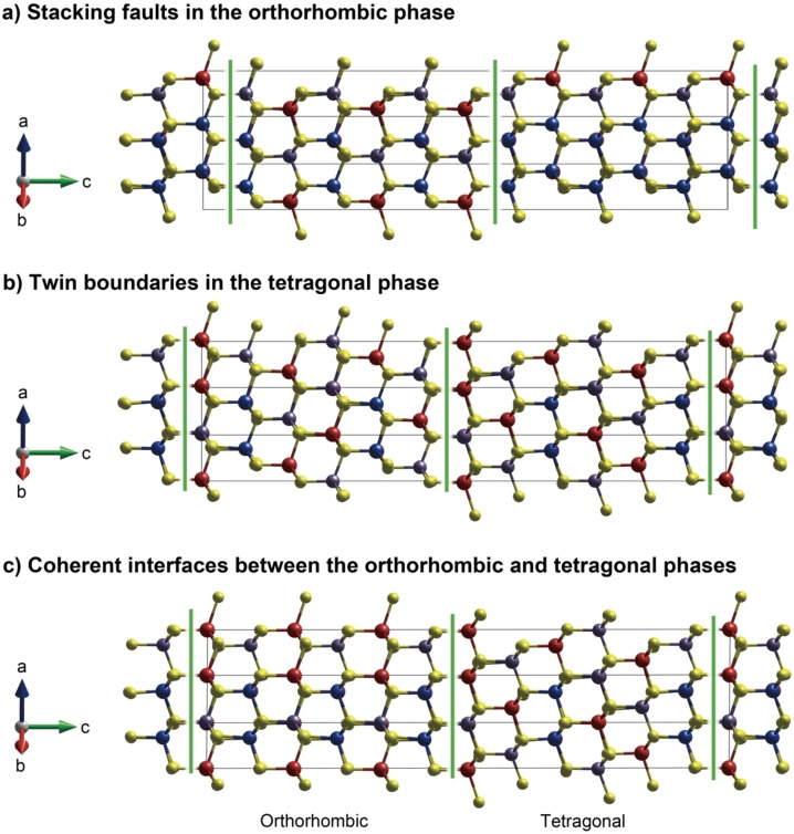
To estimate the stability of these nanoscale interfaces, ab initio calculations of the stacking faults, twin boundaries, and coherent interfaces between the orthorhombic and tetragonal phases were performed. See Figure 8 for the optimized structures of these interfaces. Their compositions were all assumed to be Cu2MnGeS4 for simplicity and sake of comparison. The results showed that these three kinds of interfaces have interface energies less than 0.003 J m−2 in absolute value. This indicates that the energetic costs by forming these interfaces are very small and are easily formed as seen in the TEM and SEM observations.
Figure 8.
Fully relaxed structures of two phases with interfaces. a) Stacking faults in the orthorhombic enargite‐type phase, b) twin boundaries in the tetragonal stannite‐type phase and c) coherent interfaces between the orthorhombic enargite‐type and tetragonal stannite‐type phases. Blue, red, gray, and yellow balls indicate Cu+, Mn2+, Ge4+ and S2− ions, respectively. The cell dimensions of these interface models are a) a=7.698 Å, b=6.560 Å, c=37.640 Å; b) a=7.730 Å, b=6.550 Å, c=37.491 Å; c) a=7.715 Å, b=6.554 Å, c=37.569 Å. Green lines are eye guides for viewing the positions of these planer defects. These structures are drawn using VESTA. [35]
Electrical and Thermal Properties
The temperature dependence of the electrical resistivity in the Cu2+x Mn1−x GeS4 series (Figure 9a) clearly show a crossover from a semiconducting to a degenerate semiconducting (SC) behavior with a decrease of the electrical resistivity by almost 3 orders of magnitude at RT as the copper content increases from x=0 to x=0.50. The pristine sample (x=0) has a semiconducting behavior with an electrical resistivity of 5 Ω cm at RT, whereas the Cu‐rich phase Cu2.5Mn0.5GeS4 exhibits a metallic‐like behavior with an electrical resistivity of 1 mΩ cm at RT. The decrease of the electrical resistivity is continuous with the increase of Cu content, the semiconducting behavior changing to a degenerate SC behavior between x=0.2 and x=0.3. It is worth pointing out that copper hyper stoichiometry was already shown to be an effective approach to increase the hole carrier concentration and to bring down the electrical resistivity over the pristine compound in different sphalerite derivative systems, such as Cu2+x Mg1−x SnSe4, Cu2+x Cd1−x SnSe4, Cu8+x Fe3−x Sn2S12, Cu2+x Sn1−x S3, Cu2+x Zn1−x GeS4, Cu2+x Fe1−x SnS4.[ 15 , 17 , 36 , 37 , 38 , 39 ] The decrease of the electrical resistivity when x increases is also probably affected by the large increase of the grain size (Figure 7). However, as the size/shape of the grains and the carrier concentration (see below) are both changing with the Cu content, it is impossible to state which factor (extrinsic or intrinsic) governs the enhancement of the electrical resistivity. Note that the measurements are thermally reversible, suggesting that the overall stoichiometry of the two phases is not significantly changed by high temperature exposure up to 700 K. However, one can notice a change of slope in all compounds around 520–550 K, except for x=0. It is especially marked for x=0.3, 0.4 and 0.5 where the sign of the slope is changing from positive to negative. To investigate the origin of this phenomenon, PXRD patterns were recorded from RT to 650 K and down to RT on x=0.3 sample (See discussion about thermal stability in Supporting Information, Figure S9).
Figure 9.
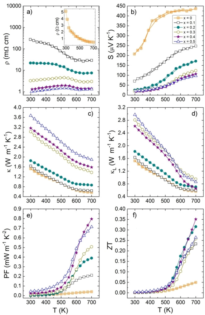
Temperature dependence of a) electrical resistivity, b) Seebeck coefficient, c) thermal conductivity, d) lattice thermal conductivity, e) power factor and f) figure of merit ZT in the Cu2+x Mn1−x GeS4 series.
The positive values of the Seebeck coefficient (Figure 9b) indicates that all the compounds are p‐type conductors. In agreement with the electrical resistivity curves, the magnitude of the Seebeck coefficient decreases with increasing x, from to 200 to 20 μV K−1 at RT. A saturation is observed for x=0.3, in agreement with the values of electrical resistivity for x=0.3, 0.4 and 0.5 samples. Considering that Ge4+ cannot participate to the electrical conduction due to the 4d 10 configuration of their orbitals, the high univalent copper content and the fact that the CuS4 tetrahedra form a 3D‐framework (Figure 1) strongly suggest that the p‐type transport properties in this sulfide material are governed by the CuI−S framework involving a hybridization of the Cu(3d 10) and S(3p 4) orbitals. In this model, the presence of hole carriers in the copper network, i.e. the mixed valence Cu2+/Cu+, is rigorously governed by the substitution of Cu for Mn. The increase of Cu content leads to an increase of the Cu2+/Cu+ ratio and consequently of the hole carrier concentration. According to the SEM‐ and STEM‐EDS analyses (Figure S7 and S8), we can assume that the increase in carrier concentration is mainly governed by the Cu enrichment in the tetragonal phase, whose content increases with x. Note that, due to the presence of two different phases and many interfaces, measured values of hole carrier concentration were not meaningful.
Figure 10a shows the element‐deconvoluted electronic DOS of orthorhombic enargite‐type Cu2MnGeS4 phase, indicating that the structure is semiconductor with the calculated band gap of about 1.0 eV. The valence band top is composed of hybridized Cu 3d and S 3p orbitals as also observed in other copper‐based sulfides. The tetragonal stannite‐type Cu2MnGeS4 phase also has an electronic structure similar to the orthorhombic enargite‐type phase, with the direct band gap of about 0.9 eV (Figures S10 and S11). On the other hand, in Cu2.5Mn0.5GeS4, the Fermi energy is shifted to the inner valence band, demonstrating that excess Cu substituted for Mn2+ sites dope holes into the top of the valence band (Figure 10b). This behavior agrees with experimental measurements where electrical resistivity and Seebeck coefficient decreases as x increases in Cu2+x Mn1−x GeS4.
Figure 10.
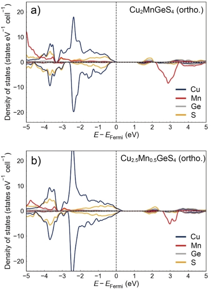
Element‐deconvoluted electronic density of states (DOS) of orthorhombic enargite‐type a) Cu2MnGeS4 and b) Cu2.5Mn0.5GeS4 phases. E Fermi indicates the Fermi energy. Positive and negative DOS indicate the partial DOS of up‐spin and down‐spin orbitals, respectively.
The increase in carrier concentration, highlighted by the decrease of the electrical resistivity and Seebeck coefficient, leads to a remarkable increase of the power factor (PF) from 0.04 mW m−1 K−2 at 700 K for x=0 to 0.8 mW m−1 K−2 for x=0.4 (Figure 9e). This maximum value is comparable to the ones reported in several Cu‐based compounds, but significantly smaller than the record value reached in colusite Cu26Cr2Ge6S32. [40]
Figure 9c shows the temperature‐dependent thermal conductivity of the series Cu2+x Mn1−x GeS4 from RT to 700 K. For all the samples, the thermal conductivity decreases monotonously with temperature, due to the increase of phonon‐phonon scattering (Umklapp process). A slight slope change is observed at around 550 K in agreement with the trend observed on the electrical resistivity curves. The thermal conductivity increases with x from 1.5 W m−1 K−1 for x=0 to 3.7 W m−1 K−1 for x=0.5 at RT. This significant increase is explained by the increase of both electronic (Figure S12) and lattice contribution to the thermal conductivity (Figure 9d). The electronic contribution is negligible for x=0 and increases to 0.7 W m−1 K−1 for x=0.5 at RT due to the decrease in electrical resistivity. The lattice thermal conductivity increases from 1.5 W m−1 K−1 to 3.0 W m−1 K−1 for x=0.5 at RT. This increase can be ascribed to both extrinsic effects (microstructure) and/or intrinsic effects (structure). According to the microstructural analysis, the increase of the lattice thermal conductivity can be mainly ascribed to the drastic grain growth with increasing Cu content, limiting the number of grain boundaries and, consequently, phonon scattering. On the other hand, anharmonic lattice dynamics calculations were performed to estimate the lattice thermal conductivity of Cu2MnGeS4 with the effects of lattice defects intentionally excluded. The calculated values of orthorhombic enargite‐type and tetragonal stannite‐type phases are approximately 3.0 and 5.1 W m−1 K−1 at RT, respectively, with most of the heat transported by low‐frequency acoustic phonons (see Figure S13 for details). The increase in lattice thermal conductivity with increasing x can be attributed to the higher lattice thermal conductivity of the tetragonal stannite‐type phase compared to the orthorhombic enargite‐type one, which originates from its higher structural symmetry and longer mean free paths of phonons.
The calculated lattice thermal conductivity for orthorhombic enargite‐type Cu2MnGeS4 (x=0) is almost double than the experimental value (1.5 W m−1 K−1 at RT). This suggests that the presence of lattice defects in these materials, namely stacking faults, nano‐twins, nano‐domains, grain boundaries and cation disordering contribute to the reduction of lattice thermal conductivity. Here, as an origin of reduced lattice thermal conductivity, we investigated the effects of nano‐interfaces (stacking faults, twins, and domains) on heat capacity and group velocity. Lattice thermal conductivity is proportional to the heat capacity and the square of group velocity, according to the kinetic theory. We modeled the interfaces with the separation of about 1.8 nm (Figure 8), which corresponds to the shortest separation between twin boundaries observed by TEM. The calculation results show that there are no significant differences in phonon DOS (heat capacity) between the interfaces and the bulk crystals (Figure S14). This is probably due to the small structural change in (Cu,Ge,Mn)S4 tetrahedra even in the vicinity of the interfaces, as also indicated from their significantly small interface energies. On the other hand, the phonon group velocities were substantially reduced from the bulk crystals (Figure S15). Especially, acoustic phonons with the frequencies below 1.5 THz, which transport most of heat, exhibit squared group velocities reduced by about 30 % as compared with those in the corresponding bulk crystals (Table S5). The decrease of group velocities indicates stationary phonons in these materials are modified, even before phonon propagations, which are found to become prominent on the nanometer scale. [41] In addition to this, the decrease in relaxation time is also expected due to lower rotational and translational symmetry of the interfacial structures. Thus, the nanoscale interfaces characterizing these materials would contribute to the reduction of lattice thermal conductivity, although the effects were overestimated in these calculations due to the higher density of interfaces than in experiments and neglect of point defects.
Lattice thermal conductivity values of pristine compound (x=0) are similar to those reported for the isostructural (orthorhombic) enargite‐type Cu3PS4 compounds with a minimum value of around 0.6 W m−1 K−1 at 700 K. [22] Such low values are mainly attributed to their small grain sizes and their similar crystal structure. The values of 1.5–2 W m−1 K−1 at 700 K determined in Cu‐rich compounds (x ≥ 0.3) are in agreement with the state‐of‐the‐art sphalerite derivative copper‐based sulfides. [3] The vibrational DOS of the tetragonal stannite‐type and orthorhombic enargite‐type phases, presented in Figure S14, exhibit similar features observed in other copper sulfides,[ 40 , 42 , 43 , 44 ] notably including a low‐frequency manifold centered at about 2 THz (≈60 cm−1) involving mostly Cu displacement. The presence of low‐energy optical modes was found in several Cu‐based sulfides with relatively low κL .
Temperature dependences of the thermoelectric figure of merit ZT in the series Cu2+x Mn1−x GeS4 are displayed in Figure 9f. Copper for Mn substitution significantly enhances the ZT values, from 0.05 for x=0 to 0.35 for x=0.4 at 700 K. This remarkable enhancement is mainly linked to the significant increase in power factor, due to an increase in carrier concentration through Cu for Mn substitution.
Conclusion
Based on the substitution of copper for manganese in the wurtzite derivative Cu2MnGeS4 compound, we have been able to synthesize a self Cu‐doped thermoelectric material Cu2+x Mn1−x GeS4. We have shown that this material prepared by low energy ball‐milling and fast SPS process cannot be described as a single phase sample or as a solid solution but as a particular biphasic system which consists of two interconnected tetrahedral frameworks at a nanoscale, with the orthorhombic enargite‐type (wurtzite derivative) and the tetragonal stannite‐type (sphalerite derivative) structures, respectively. The complex crystal chemistry of such nanocomposites rises the issue of the role of the two structures and of their interfaces in the mechanism governing their electrical and thermal conductivities. Their reasonable thermoelectric performances, reaching a ZT value of 0.35 at 700 K opens the route to future investigations in composite sulfide materials.
Conflict of interest
The authors declare no conflict of interest.
1.
Supporting information
As a service to our authors and readers, this journal provides supporting information supplied by the authors. Such materials are peer reviewed and may be re‐organized for online delivery, but are not copy‐edited or typeset. Technical support issues arising from supporting information (other than missing files) should be addressed to the authors.
Supporting Information
Acknowledgements
V.P.K and E.G. acknowledge the financial support of the French Agence Nationale de la Recherche LabEx EMC3 through the Project FACTO (Grant No. ANR‐10‐LABX‐09‐01) and FEDER. E.G. and P.L. acknowledge the financial support of CNRS through the International Emerging Actions program (EXPRESS project). S.P., P.B. and E.G. acknowledge the support from the European Union's Horizon 2020 research and innovation programme under the Marie Skłodowska‐Curie grant agreement No 956099 (NanED – Electron Nanocrystallography – H2020‐MSCA‐ITN). S.F. was supported by KAKENHI from the Japan Society for the Promotion of Science (JSPS) (Grant Nos. JP20H05195, JP20K15034). S.F., K.Y. and M.Y. were supported by KAKENHI (Grant No. JP19H05786, JP20K05062).
V. Pavan Kumar, S. Passuti, B. Zhang, S. Fujii, K. Yoshizawa, P. Boullay, S. Le Tonquesse, C. Prestipino, B. Raveau, P. Lemoine, A. Paecklar, N. Barrier, X. Zhou, M. Yoshiya, K. Suekuni, E. Guilmeau, Angew. Chem. Int. Ed. 2022, 61, e202210600; Angew. Chem. 2022, 134, e202210600.
Data Availability Statement
The data that support the findings of this study are available from the corresponding author upon reasonable request.
Crystallographic Information Files (cif files) related to the crystal structures obtained by 3D ED can be obtained from the joint CCDC/FIZ Karlsruhe online deposition service: https://www.ccdc.cam.ac.uk/structures/? by quoting the DOI of the article.
3D ED raw data will be deposited and findable in Zenodo NanED community (https://zenodo.org/communities/naned).
References
- 1. Powell A. V., J. Appl. Phys. 2019, 126, 100901. [Google Scholar]
- 2. Raveau B., J. Supercond. Novel Magn. 2020, 33, 259–263. [Google Scholar]
- 3. Lemoine P., Guélou G., Raveau B., Guilmeau E., Angew. Chem. Int. Ed. 2022, 61, e202108686; [DOI] [PubMed] [Google Scholar]; Angew. Chem. 2022, 134, e202108686. [DOI] [PubMed] [Google Scholar]
- 4. Nitsche R., Sargent D. F., Wild P., J. Cryst. Growth 1967, 1, 52–53. [Google Scholar]
- 5. Allemand J., Wintenberger M., Bull. Soc. Fr. Mineral. Cristallogr. 1970, 93, 14–17. [Google Scholar]
- 6. Bernert T., Pfitzner A., Z. Kristallogr. 2005, 220, 968–972. [Google Scholar]
- 7. Schäfer W., Nitsche R., Mater. Res. Bull. 1974, 9, 645–654. [Google Scholar]
- 8. Quintero M., Marquina J., Quintero E., Moreno E., Álvarez S., Rincón C., Grima P., Bocaranda P., Rivero D., Henao J. A., et al., Rev. Mex. Fis. 2014, 60, 168–175. [Google Scholar]
- 9. Jiang Q., Yan H., Lin Y., Shen Y., Yang J., Reece M. J., J. Mater. Chem. A 2020, 8, 10909–10916. [Google Scholar]
- 10. Isotta E., Mukherjee B., Fanciulli C., Pugno N. M., Scardi P., J. Phys. Chem. C 2020, 124, 7091–7096. [Google Scholar]
- 11. Wang B., Xiang H., Nakayama T., Zhou J., Li B., Phys. Rev. B 2017, 95, 035201. [Google Scholar]
- 12. Guan H., Hou H., Li M., Cui J., Mater. Lett. 2017, 188, 319–322. [Google Scholar]
- 13. Bourgès C., Al Rahal Al Orabi R., Miyazaki Y., J. Alloys Compd. 2020, 826, 154240. [Google Scholar]
- 14. Zhang D., Yang J., Jiang Q., Zhou Z., Li X., Xin J., Basit A., Ren Y., He X., Nano Energy 2017, 36, 156–165. [Google Scholar]
- 15. Goto Y., Naito F., Sato R., Yoshiyasu K., Itoh T., Kamihara Y., Matoba M., Inorg. Chem. 2013, 52, 9861–9866. [DOI] [PubMed] [Google Scholar]
- 16. Sarkar S., Das B., Midya P. R., Das G. C., Chattopadhyay K. K., Mater. Lett. 2015, 152, 155–158. [Google Scholar]
- 17. Heinrich C. P., Day T. W., Zeier W. G., Snyder G. J., Tremel W., J. Am. Chem. Soc. 2014, 136, 442–448. [DOI] [PubMed] [Google Scholar]
- 18. Kandare S. P., Rao M. N., Dahiwale S. S., Rao R., Dhole S. D., Chaplot S. L., J. Phys. Chem. Solids 2021, 150, 109819. [Google Scholar]
- 19. Sharma S., Kumar P., J. Phys. Commun. 2017, 1, 045014. [Google Scholar]
- 20. Nagaoka A., Masuda T., Yasui S., Taniyama T., Nose Y., Appl. Phys. Express 2018, 11, 051203. [Google Scholar]
- 21. Parthé E., Yvon K., Deitch R. H., Acta Crystallogr. Sect. B 1969, 25, 1164–1174. [Google Scholar]
- 22. Tanimoto T., Suekuni K., Tanishita T., Usui H., Tadano T., Kamei T., Saito H., Nishiate H., Lee C. H., Kuroki K., Adv. Funct. Mater. 2020, 30, 2000973–2000980. [Google Scholar]
- 23. Pfitzner A., Reiser S., Z. Krist. 2002, 217, 51–54. [Google Scholar]
- 24. Chapuis G., Niggli A., Acta Crystallogr. Sect. B 1972, 28, 1626–1628. [Google Scholar]
- 25. Quintero E., Tovar R., Quintero M., Morocoima M., Ruiz J., Delgado G., Broto J. M., Rakoto H., Phys. Condens. Matter 2002, 320, 384–387. [Google Scholar]
- 26. Dwivedi P., Miyata M., Higashimine K., Takahashi M., Ohta M., Kubota K., Takida H., Akatsuka T., Maenosono S., ACS Omega 2019, 4, 16402–16408. [DOI] [PMC free article] [PubMed] [Google Scholar]
- 27. Zhou W., Shijimaya C., Takahashi M., Miyata M., Mott D., Koyano M., Ohta M., Akatsuka T., Ono H., Maenosono S., Appl. Phys. Lett. 2017, 111, 263105. [Google Scholar]
- 28. Palatinus L., Corrêa C. A., Steciuk G., Jacob D., Roussel P., Boullay P., Klementová M., Gemmi M., Kopeček J., Domeneghetti M. C., et al., Acta Crystallogr. Sect. B 2015, 71, 740–751. [DOI] [PubMed] [Google Scholar]
- 29. Pósfai M., Sundberg M., Am. Mineral. 1998, 83, 365–372. [Google Scholar]
- 30. Treacy M. M. J., Newsam J. M., Deem M. W., Proc. R. Soc. London Ser. A 1991, 433, 499–520. [Google Scholar]
- 31. Casas-Cabanas M., Reynaud M., Rikarte J., Horbach P., Rodriguez-Carvajal J., J. Appl. Crystallogr. 2016, 49, 2259–2269. [Google Scholar]
- 32. Bourgès C., Gilmas M., Lemoine P., Mordvinova N., Lebedev O. I., Hug E., Nassif V., Malaman B., Daou R., Guilmeau E., J. Mater. Chem. C 2016, 4, 7455–7463. [Google Scholar]
- 33. Maji K., Lemoine P., Renaud A., Zhang B., Zhou X., Carnevali V., Candolfi C., Raveau B., Al Rahal Al Orabi R., Fornari M., et al., J. Am. Chem. Soc. 2022, 144, 1846–1860. [DOI] [PubMed] [Google Scholar]
- 34. Guélou G., Couder C., Bourhim A., Lebedev O. I., Daneu N., Appert F., Juraszek J., Lemoine P., Segreto L., Guilmeau E., Acta Mater. 2020, 195, 229–239. [Google Scholar]
- 35. Momma K., Izumi F., J. Appl. Crystallogr. 2011, 44, 1272–1276. [Google Scholar]
- 36. Pavan Kumar V., Guilmeau E., Raveau B., Caignaert V., Varadaraju U. V., J. Appl. Phys. 2015, 118, 155101. [Google Scholar]
- 37. Liu M.-L., Chen I.-W., Huang F.-Q., Chen L.-D., Adv. Mater. 2009, 21, 3808–3812. [Google Scholar]
- 38. Pavan Kumar V., Barbier T., Caignaert V., Raveau B., Daou R., Malaman B., Le Caër G., Lemoine P., Guilmeau E., J. Phys. Chem. C 2017, 121, 16454–16461. [Google Scholar]
- 39. Deng T., Qiu P., Song Q., Chen H., Wei T., Chen L., Xi L., Shi X., Chen L., J. Appl. Phys. 2019, 126, 085111. [Google Scholar]
- 40. Pavan Kumar V., Supka A. R., Lemoine P., Lebedev O. I., Raveau B., Suekuni K., Nassif V., Al Rahal Al Orabi R., Fornari M., Guilmeau E., Adv. Energy Mater. 2019, 9, 1803249. [Google Scholar]
- 41. Fujii S., Funai K., Yokoi T., Yoshiya M., Appl. Phys. Lett. 2021, 119, 231604. [Google Scholar]
- 42. Bourgès C., Bouyrie Y., Supka A. R., Al Rahal Al Orabi R., Lemoine P., Lebedev O. I., Ohta M., Suekuni K., Nassif V., Hardy V., et al., J. Am. Chem. Soc. 2018, 140, 2186–2195. [DOI] [PubMed] [Google Scholar]
- 43. Hagiwara T., Suekuni K., Lemoine P., Supka A. R., Chetty R., Guilmeau E., Raveau B., Fornari M., Ohta M., Al Rahal Al Orabi R., et al., Chem. Mater. 2021, 33, 3449. [Google Scholar]
- 44. Deng T., Xing T., Brod M. K., Sheng Y., Qiu P., Veremchuk I., Song Q., Wei T.-R., Yang J., Snyder G. J., et al., Energy Environ. Sci. 2020, 13, 3041–3053. [Google Scholar]
Associated Data
This section collects any data citations, data availability statements, or supplementary materials included in this article.
Supplementary Materials
As a service to our authors and readers, this journal provides supporting information supplied by the authors. Such materials are peer reviewed and may be re‐organized for online delivery, but are not copy‐edited or typeset. Technical support issues arising from supporting information (other than missing files) should be addressed to the authors.
Supporting Information
Data Availability Statement
The data that support the findings of this study are available from the corresponding author upon reasonable request.
Crystallographic Information Files (cif files) related to the crystal structures obtained by 3D ED can be obtained from the joint CCDC/FIZ Karlsruhe online deposition service: https://www.ccdc.cam.ac.uk/structures/? by quoting the DOI of the article.
3D ED raw data will be deposited and findable in Zenodo NanED community (https://zenodo.org/communities/naned).


