Abstract
The relationship between the structure and properties of materials is the core of material research. Bulk Pd3(PS4)2 materials have been successfully synthesized in the field of three-dimensional materials. After that, various studies on two-dimensional layered materials were conducted. Inspired by these successes, this work used density functional theory based on first principles to explore similar two-dimensional Pd3(AsX4)2, where X is S, Se, or Te belonging to the same group. Our findings demonstrate that the Pd3(AsS4)2 and Pd3(AsSe4)2 monolayers, with HSE06 band gaps of 2.37 and 1.36 eV, respectively, are indirect semiconductors. Additionally, their carrier mobilities [523.23 cm2 s−1 V−1 and 440.6 cm2 s−1 V−1] are also proved to be superior to MoS2 [∼200 cm2 s−1 V−1]. The optical calculations indicate that the Pd3(AsSe4)2 monolayer yields suitable valence band edge positions for the visible-light-driven water splitting reactions. More interestingly, at a low applied voltage of 0.14 V, Pd3(AsSe4)2 exhibits outstanding oxygen evolution reaction performance. In this study, the possible mechanism for the ability of Pd3(AsSe4)2 monolayer to promote photocatalysis and oxygen evolution was explained, which may pave the way for the practical design of further solar-driven high-quality water splitting photocatalysis.
The relationship between the structure and properties of materials is the core of material research.
Introduction
To address the environmental issues brought by the combustion of fossil fuels that significantly alleviated the energy crisis, research on renewable clean energy, such as solar energy, has sparked a boom in the field of materials science and chemistry.1,2 Therefore, the search for two-dimensional (2D) materials that can serve as highly effective photovoltaic (PV) solar cells and water splitting catalysts present an attractive prospect for providing clean and sustainable energy without burning fossil fuels or releasing chemical pollutants.3–6 Many materials have been identified as having photocatalytic potential7–11 since the first TiO2 photocatalytic water splitting demonstration by Fujishima and Honda in 1972.12 Two half-reactions, the oxygen evolution reaction (OER) and hydrogen evolution reaction (HER), where OER is a four-electron process and HER is a two-electron process, make up the entire process of photocatalytic water splitting. As a result, OER is more complicated than HER and is typically regarded as the step reaction process that determines the rate throughout the entire water splitting process.13,14 Research on 2D materials has entered a period of rapid development ever since Novoselov and Geim successfully synthesized monolayer graphene in 2004, which showed exceptional physical properties, such as enormous specific surface area and high carrier mobility.15 These characteristics also make 2D materials suitable for a variety of electronic,16–19 optoelectronic,20–23 and plasma devices.24–26
For photocatalytic water decomposition and oxygen evolution, 2D materials, such as g-C3N4 (0.43 V),27 β-GeSe (0.497 V),9 and TlPt2S3 (2.46 V),11 have been reported to be excellent catalysts. However, the disadvantage is that these materials require a considerable amount of additional voltage. Therefore, in order to solve the issue of increasing energy demand in the future, it is crucial to investigate 2D semiconductor materials with proper band gaps and low reaction voltages for oxygen evolution.
Palladium thiophosphate (Pd3(PS4)2), the layered crystal, was initially synthesized in 1971 by Bither et al.28 Later, through theoretical investigations, Jing and Tang et al. discovered that 2D layered Pd3(PS4)2 has excellent photocatalytic water splitting capabilities.29–32 Given that both P and As atoms are in group-VA of the periodic table, while S, Se, and Te atoms are in group-VIA, substituting atoms of the same group in similar configurations may result in similar or even better properties. Inspired by this, in this study, we investigated the dynamical stability, mechanical, electronic, and photocatalytic water splitting properties of Pd3(AsX4)2 (X = S, Se, and Te) monolayers using the density functional theory (DFT) calculations.
Computational details
Our DFT computations were performed using the Vienna ab initio simulation package (VASP),33 and the projector augmented wave (PAW)34 method was utilized to describe the ion–electron interactions. The Perdew–Burke–Ernzerhof functional (PBE)35 within the generalized gradient approximation (GGA) was used throughout our computations. A hybrid functional based on the Heyd–Scuseria–Ernzerhof (HSE06) exchange–correlation functional36 was adopted for accurately calculating the band structure and absorption properties. The energy cut-off of the plane waves was set to 400 eV. The structures were fully relaxed until the maximum force on each atom was less than 0.005 eV Å−1, and the energy convergence criterion in the self-consistent calculations was set to 10−5 eV. The 4 × 4 × 1 and 8 × 8 × 1 Monkhorst–Pack k-point grids were used for geometry optimizations and self-consistent calculations, respectively. A vacuum region of at least 20 Å in the z direction was adopted to avoid artificial interactions between the neighboring layers. The phonon dispersion was calculated using the Phonopy code37 within the density functional perturbation theory (DFPT).38 In phonon calculations, a supercell is used with 2 × 2 × 1 and an atomic displacement distance of 0.01 Å. A finer k-point grid of 2π × 0.02 Å−1 was employed. To further confirm the thermal stability of the 2D Pd3(AsX4)2 (X = S, Se, and Te) monolayers, the ab initio molecular dynamics (AIMD) simulation within the canonical ensemble (NVT) and Nosé–Hoover thermostat at 300 K and 500 K were carried out on a 3 × 3 × 1 supercell. At each temperature, the AIMD simulation in the NVT ensemble lasted for 5 ps with a time step of 1.0 fs.
For the investigation of optical properties, according to the following expression, the light absorption coefficients of the structures are calculated:39 Thus, in the dielectric equation, ε1 and ε2 stand for the real and imaginary parts, respectively. In this, the contribution of inter-band transition is used to calculate ε2:40
 where Ω expresses the unit cell volume. q is the Bloch vector of the incident wave. wk is the k-point weight. c and v represent the conduction band state and the valence band state, respectively. uck represents the cell periodic part of the orbitals at point k. Kramers–Kronig transformation was used to determine the real part ε1:40
 where P is the principle value. η denotes the complex shift in the Kramers–Kronig transformation.
We simulated the OER reaction under the neutral condition of pH = 7 and temperature for 300 K in order to quantify the performance of the OER and understand the underlying photocatalytic mechanism. The expressions below illustrate how this procedure can be broken down into four phases:41* + H2O → *OH + H+ + e−*OH → *O + H+ + e−*O + H2O → *OOH + H+ + e−*OOH → * + O2 + H+ + e−where * denotes a free position on the surface that can be adsorbed, and *OH, *O, and *OOH denote the OH, O, and OOH intermediates adsorbed on the surface, respectively.
We used a method established by Nørskov et al.42 to calculate the free energy change (ΔG) in the water oxidation reactions. This method states that the ΔG of an electrochemical reaction is computed asΔG = ΔE +ΔEZPE − TΔS + ΔGU + ΔGpHwhere ΔE is the adsorption energy, ΔEZPE, and ΔS are the differences in zero point energy and entropy difference between the adsorbed state and the gas phase, respectively. We used a finite difference method to calculate the vibration frequencies of all adsorbed species for entropy and zero-point energy.43T stands for the ambient temperature (300 K). The free energy contributed in different pH concentrations is represented by ΔGpH (ΔGpH = kBT × ln 10 × pH). ΔGU (ΔGU = −eU) signifies extra potential bias produced by an electron in the electrode, where U represents the electrode potential with respect to the standard hydrogen electrode (SHE).
Results and discussion
Structures and stabilities
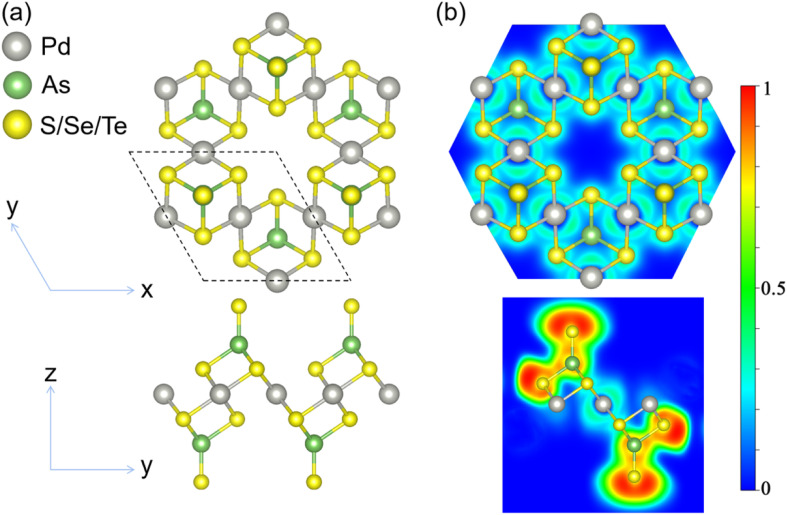
We first explored 2D Pd3(AsX4)2 compounds with lattice structures similar to that of Pd3(PS4)2. For X covering the group-VIA elements (S, Se, and Te). Fig. 1 depicts the monolayer Pd3(AsX4)2 (X = S, Se, and Te) crystal structure. The optimized lattice parameters are a = b = 6.882 (7.180 and 7.569) Å for the Pd3(AsX4)2 (X = S, Se, and Te) monolayers, which crystallize in the P3̄m1 space group. Due to the varying radii of various atoms, the lattice constants of the Pd3(AsX4)2 (X = S, Se, Te) monolayers are slightly larger than that of the Pd3(PS4)2 (a = b = 6.64 Å) monolayer.30 The detailed structural information of the three layers is listed in Table 1. We calculated the electron localization function (ELF) to describe the bonding behavior in the structure. As shown in Fig. 1b, electrons are primarily localized between As–X (X = S, Se, and Te) atoms. In contrast, there are no electron localizations between the X–Pd (X = S, Se, and Te) atoms. The above results reflect the covalent bonding states between the As and X (X = S, Se, and Te) atoms and the ionic bonding between X (X = S, Se, and Te) and Pd atoms.
Fig. 1. (a) Atomic structure of the Pd3(AsX4)2 (X = S, Se, and Te) monolayer. The dashed line represents the primitive cell. (b) The electron localization function (ELF). The isosurface for ELF is 0.75e Å−3.
Lattice parameter Lp (in Å), space group, cohesive energy Ecoh (in eV per atom), and formation energy ΔHf (in eV per atom) for monolayers Pd3(AsX4)2 (X = S, Se, Te).
| Phase | L p | Space group | E coh | ΔHf |
|---|---|---|---|---|
| Pd3(AsS4)2 | a = b = 6.882 | P3̄m1 | −4.28 | −4.18 |
| Pd3(AsSe4)2 | a = b = 7.180 | P3̄m1 | −3.74 | −3.18 |
| Pd3(AsTe4)2 | a = b = 7.569 | P3̄m1 | −3.56 | −3.53 |
To assess the thermodynamic stabilities of the Pd3(AsX4)2 (X = S, Se, Te) monolayers, we first calculated their cohesive energy using the following equation:Ecoh = [E(PdxAsyXz) − xE(Pd) − yE(As) − zE(X)]/(x + y + z)where x, y, and z represent the number of atoms in the cell, E(PdxAsyXz) is the total energy of the Pd3(AsX4)2 (X = S, Se, and Te) layers, E(Pd), E(As), and E(X) are the energies of the isolated Pd, As, and X atoms, respectively. A more negative Ecoh value, by this definition, denotes higher thermodynamic stability. Pd3(AsS4)2, Pd3(AsSe4)2, and Pd3(AsTe4)2 monolayers have computed cohesive energies of −4.28, −3.89, and −3.56 eV per atom, respectively, which are lower than those of Cu2Si (−3.46 eV per atom),44 silicene (−3.98 eV per atom),44 and germanene (−3.26 eV per atom)44 monolayers at the same theoretical level, and the cohesive energy of Pd3(AsS4)2 is equivalent to that of the Pd3(PS4)2 (−4.55 eV per atom) monolayer. The relatively small cohesive energies of 2D Pd3(AsX4)2 compounds suggest that the monolayers are stable phases of Pd–X–As systems. We should note, especially for the compound, which has not yet been synthesized, the negative values of the cohesive and formation energies are necessary. Next, we calculated the formation energy of the Pd3(AsX4)2 monolayers. The formation energy (ΔHf) is defined as the difference between the energy of a crystal and corresponding constituent elements in their standard states. The formation energy is given by the following expression:ΔHf = [E(PdxAsyXz) − xμ(Pd) − yμ(As) − zμ(X)]/(x + y + z)where x, y, and z represent the number of atoms in the cell, E(PdxAsyXz) is the total energy of the Pd3(AsX4)2 (X = S, Se, and Te) layers. μ(Pd), μ(As), and μ(X) are the chemical potentials of Pd, As, and X (X = S, Se, and Te), respectively. For most elements, chemical potentials are equal to the DFT total energies of their ground states.45Table 1 provides the obtained values of ΔHf. The negative values of the formation energies of Pd3(AsX4)2 (X = S, Se, and Te) monolayers indicate the stability of these compounds. For a material to be thermodynamically stable, it is necessary but not sufficient that ΔHf < 0. Indeed, thermodynamic stability requires that ΔHf be negative not only relative to its pure elemental phases but relative to all other competing phases, i.e., its energy must be below the convex hull.46 Thus, we calculated the energy above the convex hull (ΔHhull) by using the following formula,ΔHhull = ΔHf − ΔHwhere ΔHf is the formation energy of the Pd3(AsX4)2 (X = S, Se, and Te) monolayers, ΔH is the convex hull energy at the Pd3(AsX4)2 (X = S, Se, and Te) composition. When ΔHhull < 0, it indicates that the structure is thermodynamically stable. By calculation, we found that the ΔHhull of the Pd3(AsS4)2 structure is 0.02 eV per atom. Due to the DFT-related uncertainty/calculation error problem, ΔHhull can be considered thermodynamically stable at less than 0.025 eV per atom.45 Therefore, it is thermodynamically stable for the Pd3(AsS4)2 monolayer. Similarly, we calculated the two structures Pd3(AsSe4)2 and Pd3(AsTe4)2 and found that the ΔHhull for the Pd3(AsSe4)2 structure is 0.03 eV per atom, which is very close to 0.025 eV per atom. Therefore, the Pd3(AsSe4)2 structure is also considered to be thermodynamically stable. However, the Pd3(AsTe4)2 structure has energy above the convex hull of as high as 0.3 eV per atom, indicating that it is thermodynamically unstable. So, the Pd3(AsTe4)2 structure is not sufficient to establish its experimental growth. Therefore, we further explored the other stability of the Pd3(AsX4)2 (X = S, Se, and Te) structure.
Based on the elastic stability criteria,47 stable 2D Pd3(AsX4)2 (X = S, Se, and Te) lattices should satisfy C11, C22, C66 > 0 and C11C22 > C122, where Cij are the elastic constants. The summarized values shown in Table S1† indicate that the criteria are fully satisfied. Then, as shown in Fig. 2a–c, we calculated the phonon dispersion along the high-symmetry lines in the first Brillouin zone to assess the dynamical stabilities of Pd3(AsX4)2 (X = S, Se, and Te) monolayers. There is not any appreciable imaginary frequency in the phonon spectrum of these Pd3(AsX4)2 (X = S, Se, and Te) monolayers, suggesting the dynamical stabilities of these different structures.
Fig. 2. (a–c) Phonon dispersions of Pd3(AsS4)2, Pd3(AsSe4)2 and Pd3(AsTe4)2 monolayers, respectively.
We further performed AIMD simulations to evaluate the thermal stabilities of Pd3(AsX4)2 (X = S, Se, and Te) monolayers. We used a relatively large 3 × 3 supercell and carried out AIMD simulations at the temperatures of 300 K and 500 K for Pd3(AsX4)2 (X = S, Se, and Te) monolayers. The energy of monolayers Pd3(AsX4)2 (X = S and Se) changes only in a small range (∼0.1 eV per atom), as shown in Fig. S1 of the ESI,† and its structure can be successfully preserved through the simulation time. For the Pd3(AsTe4)2 monolayer, however, the structure collapses after the simulation, making it unstable at ambient temperature, which is consistent with the results of ΔHhull. Thus, in the following discussion, we will mainly focus on Pd3(AsS4)2 and Pd3(AsSe4)2 monolayers. After that, we performed AIMD simulations of the Pd3(AsS4)2 and Pd3(AsSe4)2 monolayers at 500 K, as shown in Fig. S2 of the ESI.† At the end of the simulations, we found that both the structures could still be maintained and the energy fluctuated in a small range, as shown in Fig. S2 of the ESI.† Meanwhile, we investigated the chemical stability of Pd3(AsS4)2 and Pd3(AsSe4)2 monolayers, which is the capacity of 2D materials to preserve their original physical and chemical properties in the environment. We used the surface work function to evaluate the chemical stability of the monolayers Pd3(AsS4)2 and Pd3(AsSe4)2.48 Their physical meaning is described as the essential energy to remove an electron from the Fermi level. A low work function means that the electrons are loosely bound, which is advantageous for carrier transfer during the photocatalytic process but detrimental to the chemical stability of the material.9 Here, we merely take into account the work function of the vacuum environment monolayers of Pd3(AsS4)2 and Pd3(AsSe4)2. The monolayers Pd3(AsS4)2 and Pd3(AsSe4)2 (5.5 and 5.43 eV) have greater work functions than black phosphorene (4.50 eV),49 as illustrated in Fig. S3,† demonstrating their exceptional chemical stability. The Pd3(AsS4)2 and Pd3(AsSe4)2 monolayers are energetically, dynamically, thermally, and chemically stable, according to these systematic studies.
Electronic and transport properties
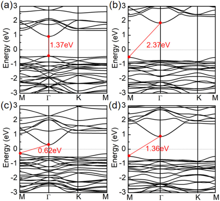
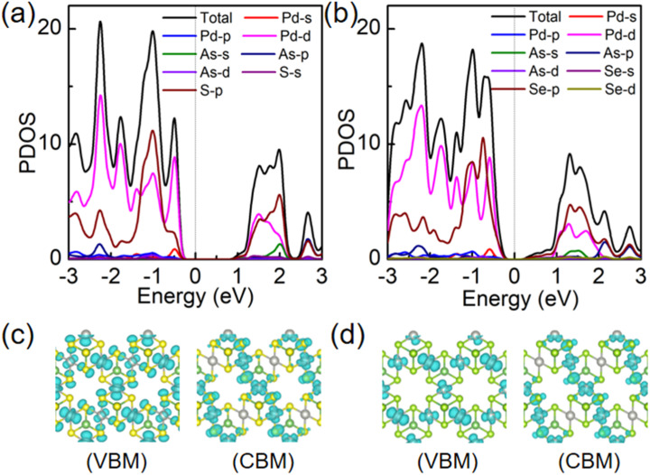
We will now look into their electronic properties. Based on band structure calculations using the PBE method, it was found that the Pd3(AsS4)2 and Pd3(AsSe4)2 monolayers are direct and indirect semiconductors with a band gap of 1.37 eV and 0.68 eV, respectively. The valence band maximum (VBM) and conduction band minimum (CBM)of the Pd3(AsS4)2 monolayer are both located at the Γ point. However, for the Pd3(AsSe4)2 monolayer, the VBM is at the M point, while CBM is at the Γ point, as illustrated in Fig. 3a and c. The projected density of states (PDOS) on the atomic orbitals is also shown in Fig. 4a and b. It is evident that the d orbital of Pd and p orbital of S (Se) both make a major contribution to the Fermi energy and exhibit a certain orbital hybridization effect. The electronic states of CBM and VBM in Pd3(AsS4)2 and Pd3(AsSe4)2 monolayers are also studied in order to better investigate the charge distribution of Pd3(AsS4)2 and Pd3(AsSe4)2 monolayers. For the Pd3(AsS4)2 monolayer, as shown in Fig. 4c and d, VBM demonstrates that electrons are localized around all Pd atoms and some S atoms, while CBM comes from all S atoms and some Pd atoms. In contrast to the Pd3(AsS4)2 monolayer, the VBM of the Pd3(AsSe4)2 monolayer exhibits a concentration of all electrons around Pd atoms, whereas the CBM contains both Pd atoms and Se atoms. These findings are in line with the results of the PDOS results on Pd3(AsS4)2 and Pd3(AsSe4)2 monolayers.
Fig. 3. Band structures of Pd3(AsS4)2 and Pd3(AsSe4)2 monolayers by the (a and c) PBE and (b and d) HSE06 methods.
Fig. 4. Projected density of states (PDOS) of (a) Pd3(AsS4)2 and (b) Pd3(AsSe4)2 monolayers by the PBE method. Partial charge density distributions of the VBM and CBM for (c) Pd3(AsS4)2 and (d) Pd3(AsSe4)2 monolayers by the PBE method. The isosurface is set to be 0.006e Å−3.
It is well-known that the PBE functional generally underestimates the band gap by about 30%;50 we thus carried out the hybrid density functional (HSE06) calculations to achieve a more accurate band gap. The band gaps of Pd3(AsS4)2 and Pd3(AsSe4)2 monolayers are 2.37 eV (Fig. 3b) and 1.36 eV (Fig. 3d), respectively, according to the HSE06 calculations. The direct band gap of the Pd3(AsS4)2 monolayer becomes an indirect band gap at this time. At the same time, we also analyzed the PDOS by using the HSE06 method, as shown in Fig. S4.† We found that the HSE06 results are generally consistent with the PBE results. The activity and water-splitting efficiency of a photocatalyst are greatly influenced by the band gap and the electronic band structure. As previously reported, the band gap should be between 1.23 eV and 3.00 eV, in order to realize an efficient light-harvesting photocatalyst for water splitting.51 Pd3(AsX4)2 (X = S and Se) monolayers perfectly satisfy this criterion because they have band gap values of 2.37 and 1.36 eV, respectively.
The efficiency of photocatalysis will decline if the rate of electrons and hole recombination is high. Two-dimensional materials, which have a low dimension and a high rate of carrier migration compared to three-dimensional ones, are better equipped to prevent the compounding of photo electron–hole pairs. An increase in carrier mobility leads to higher photocatalytic efficiency as it allows for faster transport to the photocatalyst surface. Moreover, it is preferable to suppress the recombination of electrons and holes, which can be achieved by the difference between electron and hole mobilities in the same direction.52
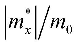
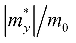
Therefore, to illustrate the carrier mobilities along the x and y directions, rectangular lattices (Fig. S5†) were used. The effective masses of carriers, which depend on the band structure of the region around the band edges, were determined by fitting a linear function to the CBM (electrons) and VBM (holes) using the following equation: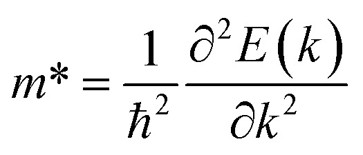 where E(k) represents the energy at the band boundaries as a function of wave number k. Table 2 displays the results obtained for the carrier effective mass m*.
Calculated effective mass |m*|, DP constant |E1|, in-plane stiffness C2D (in N m−1), carrier mobility μ (cm2 s−1 V−1) for Pd3(AsS4)2 and Pd3(AsSe4)2 monolayers along the x and y directions.
| Phase | Carrier type |
|
|
|E1x| | |E1y| | C 2Dx | C 2Dy | μ x | μ y | |
|---|---|---|---|---|---|---|---|---|---|---|
| Pd3(AsS4)2 | Hole | 9.32 | 12.97 | 3.43 | 3.44 | 14.5 | 13.0 | 0.198 | 0.092 | |
| Electron | 1.05 | 1.00 | 0.59 | 0.81 | 523.23 | 280.75 | ||||
| Pd3(AsSe4)2 | Hole | 1.15 | 1.60 | 2.31 | 3.32 | 10.3 | 9.9 | 2.166 | 12.72 | |
| Electron | 1.64 | 1.36 | 0.56 | 0.41 | 168.55 | 440.6 | ||||
The in-plane stiffness (C2D) can be calculated by simulating the total energy (E) change of the applied strain (ε) motivated by the 2D materials with the equation C2D = [∂2E/∂ε2]/S0, where S0 is the surface area of the optimized supercell. The linear relationship between the band edge for VBM and CBM and the strain exertion (ε) along the x and y direction, respectively, was fitted to estimate the Deformation Potentials (DP) constant (E1).
According to the DP theory, the following expression can be used to determine the carrier mobility of 2D materials,53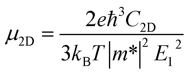 Here, ℏ is the reduced Planck constant, kB is the Boltzmann constant, and T is the temperature (set to be 300 K). The carrier mobilities of Pd3(AsS4)2 and Pd3(AsSe4)2 monolayers along different directions can be calculated by a straightforward application of the expression above because C2D, m* as well as E1 have already been estimated. The calculated carrier mobilities are listed in Table 2. The electron carrier mobility of Pd3(AsS4)2 and Pd3(AsSe4)2 are 523.23 cm2 s−1 V−1 and 440.6 cm2 s−1 V−1, respectively, which are significantly higher than those of MoS2 [∼200 cm2 s−1 V−1]54 and GeP3 [∼190 cm2 s−1 V−1].55 The hole carrier mobility of Pd3(AsS4)2 and Pd3(AsSe4)2 are 0.198 and 12.72 cm2 s−1 V−1, respectively, indicating that they are both electron-transport semiconductors. Such high electron carrier mobilities make it possible for carriers to migrate rapidly to the surface. The large difference of electron and hole mobilities in the same direction can effectively suppress the recombination of the photo-generated electron–hole pairs, thus effectively improving the photocatalytic performance of Pd3(AsS4)2 and Pd3(AsSe4)2.
Strain effect on the electronic property
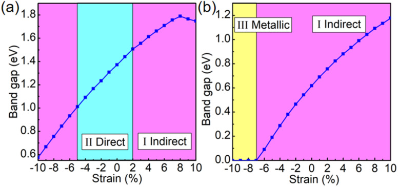
Previous studies have shown that external strain can have a significant impact on the electronic and optical properties of materials.56,57 In actuality, the substrates that are employed to support the 2D materials make strain effects inescapable. We found that these 2D materials have excellent mechanical properties, as shown in Fig. S6.† The strain–stress diagram S6† shows that the Pd3(AsS4)2 and Pd3(AsSe4)2 monolayers can maintain the ideal strain of 48% and 50%, respectively, which is much larger than that of other well-known 2D materials such as molybdenum disulfide (20%)58 and graphene (24%),59 indicating the high mechanical strength and excellent mechanical properties of the Pd3(AsS4)2 and Pd3(AsSe4)2 monolayers. New insights into the applications of flexible electrical and photonic devices will be revealed by the modulation of the band gap and electronic structure by strain. Using the PBE functional, the band gap as a function of the biaxial strain is plotted in Fig. 5. Based on the different band structures, two strain zones can be distinguished with clarity. For the Pd3(AsS4)2 monolayer, zone I is for an indirect band gap with a strain range of 2–10%, where the band gap initially increases and reaches its maximal value of 1.79 eV at 8% strain before rapidly decreasing with further expansion. It should be noted that increasing the strain up to 10% (gap, 1.75 eV) will not cause the gap to disappear completely. Nevertheless, 2D Pd3(AsS4)2 transforms into a direct band gap semiconductor in the strain range of −5 to 2% (zone II). The direct band gap, however, transforms into an indirect band gap when the strain hits −5%, and when the compressive strain reaches 10%, the band gap still does not go away completely. As a result, the Pd3(AsS4)2 monolayer exhibits semiconductor characteristics in the strain range of −10 to 10% (Fig. 5a). For the Pd3(AsSe4)2 monolayer, zone I corresponds to an indirect band gap with the strain ranging from −7 to 10%, where the band gap is gradually increased. It should be observed that increasing the strain up to 10% (gap, 1.18 eV) is not able to make the gap disappear, and stretching the material results in no band gap transition. Most interestingly, zone III demonstrates that the Pd3(AsSe4)2 monolayer's band gap decreases to zero when the compressive strain exceeds −7% and the material transforms into a metal (Fig. 5b). Fig. S7† illustrates that the semiconductor-to-metal transition is caused by the downward shift of the CBM and an upward movement of VBM, for the monolayer Pd3(AsSe4)2. The change in band gap suggests that the semiconductor can be tailored for specific electronic applications.
Fig. 5. Band gaps of the (a) Pd3(AsS4)2 and (b) Pd3(AsSe4)2 monolayers as a function of biaxial strain based on the PBE calculations. Zones I, II, and III correspond to the indirect band gap, direct band gap, and metallic properties, respectively.
Photocatalytic properties
To evaluate the potential of the material for photocatalysis, it is necessary to investigate its optical characteristics and determine whether it meets the required band gap.
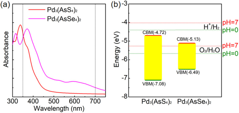
In the visible light region (350–700 nm),60 we found that only the Pd3(AsSe4)2 structure exhibits high absorption efficiency, while the absorption efficiency of the Pd3(AsS4)2 structure is poor, indicating that Pd3(AsSe4)2 has a greater potential for photocatalytic applications (Fig. 6a).
Fig. 6. (a) Light absorption spectra of Pd3(AsS4)2 (red line) and Pd3(AsSe4)2 monolayers (magenta line) calculated by the HSE06 method. (b) Band edge alignment for water redox reactions of Pd3(AsS4)2 (red line) and Pd3(AsSe4)2 at pH = 0 and 7.
The energy levels of the VBM and CBM must, respectively, be lower and greater than the water oxidation and reduction potential levels in order to satisfy the conditions for spontaneous water splitting. The water oxidation potential and reduction potential are also dependent on the pH and can be expressed by the following equations:61,62EO2/H2OOER = −5.67 + pH × 0.059 eVEH+/H2HER = −4.44 + pH × 0.059 eV
Therefore, for O2/H2O and H+/H2 at pH = 0 (pH = 7), respectively, the potential of the standard oxidation and reduction potentials relative to the vacuum level is −5.67 (−5.26) and −4.44 (−4.03) eV. The positions of VBM and CBM of Pd3(AsS4)2 and Pd3(AsSe4)2 in relation to vacuum level are depicted in Fig. 6b, respectively.
The results demonstrated that Pd3(AsSe4)2 monolayer is a promising photocatalyst for OER under visible light irradiation. This is because the VBM is lower than −5.67 eV and the material has good absorption efficiency in the visible light region.
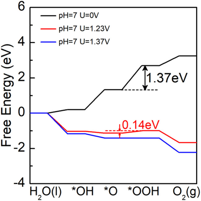
We built a 2 × 2 supercell with 12 Pd, 8 As, and 32 Se atoms for the Pd3(AsSe4)2 single-layer. The potential adsorption sites are all thought to be the Pd and Se atoms (Fig. S8†). We discovered that the active site is situated at the Se2 atom, according to the calculation. The atomic configurations of the intermediates along the water oxidation reaction pathway on the Pd3(AsSe4)2 monolayer are shown in Fig. S9,† and the related free-energy profiles under the neutral condition (pH = 7) are summarized in Fig. 7. The black line represents the Gibbs free energy change of the OER for the Pd3(AsSe4)2 monolayer when no voltage is applied (U = 0 V), the red line represents the change in Gibbs free energy for the Pd3(AsSe4)2 monolayer when exposed to light conditions (U = 1.23 V), and the blue line is the change in Gibbs free energy for the Pd3(AsSe4)2 monolayer when the minimum voltage required is applied (U = 1.37 V).
Fig. 7. Gibbs free-energy (ΔG) diagrams for OER on Pd3(AsSe4)2 at various electrode potentials.
From Fig. 7, we can see that in the third step, the highest Gibbs free energy (∼1.37 eV) is required to oxidize O* species to OOH* species. The photocatalytic oxygen evolution reaction of Pd3(AsSe4)2 can proceed smoothly when a voltage of 0.14 V is applied under the light condition of pH = 7. Experimentally, the applied voltages for Pd3(AsSe4)2 are feasible, and they are also considerably lower than those for g-C3N4 (0.43 V),27 Ni/graphene composite (0.35 V),63 C2N-based type-II heterojunctions (C2N/GaTe: 1.47 V, C2N/InTe: 0.94 V),64 numerous TM@C catalysts or metal oxides (0.49–1.7 V),65 and the extensively researched catalyst γ(Ni, Fe)OOH (0.56 V).66 It suggests that the Pd3(AsSe4)2 has the potential to be an outstanding photocatalyst for water splitting to oxygen evolution.
Conclusions
Motivated by the reports on the synthesis of 2D Pd3(PS4)2, an extensive first-principles analysis was carried out to investigate the physical properties of the Pd3(AsX4)2 (X = S, Se, Te) monolayers. It is demonstrated that the Pd3(AsX4)2 (X = S, Se) monolayers under consideration are dynamical, thermodynamic, chemical, and mechanical stability. By using the HSE06 method, we have shown that Pd3(AsX4)2 (X = S and Se) monolayers are electron-transport semiconductors with indirect bandgaps of 2.37 eV and 1.36 eV, respectively. They have high carrier mobility of 523.23 cm2 s−1 V−1 and 440.6 cm2 s−1 V−1, respectively, which are significantly higher than that of MoS2 [∼200 cm2 s−1 V−1]. More specifically, the Pd3(AsSe4)2 monolayer exhibits good light absorption in the visible light region. Finally, Pd3(AsSe4)2 was proven to be a potential photocatalytic OER catalyst. These findings suggest that the Pd3(AsSe4)2 monolayer could be a promising material for the development of efficient photocatalysts for water-splitting applications.
Conflicts of interest
There are no conflicts to declare.
Supplementary Material
Acknowledgments
This work was supported by the National Natural Science Foundation of China (Grant No. 12164050 and 12264022), Major Science and Technology Project of Precious Metal Materials Genetic Engineering in Yunnan Province (Grant No. 2019ZE001-1, 202002AB080001-6, 2018IC058), Program for Yunling Scholars in Yunnan Province, Program for Donglu Scholars in Yunnan University, Project of the Science Research foundation of the Department of Education in Yunnan Province.
Electronic supplementary information (ESI) available. See DOI: https://doi.org/10.1039/d3ra00592e
References
- Guo S. Li X. Li J. Wei B. Nat. Commun. 2021;12:1343. doi: 10.1038/s41467-021-21526-4. [DOI] [PMC free article] [PubMed] [Google Scholar]
- Jeong M. Choi I. W. Go E. M. Cho Y. Kim M. Lee B. Jeong S. Jo Y. Choi H. W. Lee J. Bae J.-H. Kwak S. K. Kim D. S. Yang C. Science. 2020;369:1615–1620. doi: 10.1126/science.abb7167. [DOI] [PubMed] [Google Scholar]
- Maeda K. Domen K. J. Phys. Chem. Lett. 2010;1:2655–2661. [Google Scholar]
- Li X. Li Z. Yang J. Phys. Rev. Lett. 2014;112:018301. doi: 10.1103/PhysRevLett.112.018301. [DOI] [PubMed] [Google Scholar]
- Zhou T. Cao Z. Zhang P. Ma H. Gao Z. Wang H. Lu Y. He J. Zhao Y. Sci. Rep. 2017;7:46154. doi: 10.1038/srep46154. [DOI] [PMC free article] [PubMed] [Google Scholar]
- Dahan M. H. Caspary Toroker M. J. Phys. Chem. C. 2017;121:6120–6125. [Google Scholar]
- Lv L. Shen Y. Liu J. Gao X. Zhou M. Zhang Y. Meng X. Yang X. Gong D. Zheng Y. Zhou Z. Appl. Surf. Sci. 2022;600:154055. [Google Scholar]
- Singh A. K. Mathew K. Zhuang H. L. Hennig R. G. J. Phys. Chem. Lett. 2015;6:1087–1098. doi: 10.1021/jz502646d. [DOI] [PubMed] [Google Scholar]
- Xu Y. Xu K. Ma C. Chen Y. Zhang H. Liu Y. Ji Y. J. Mater. Chem. A. 2020;8:19612–19622. [Google Scholar]
- Zhang Y. Shen Y. Liu J. Lv L. Gao X. Zhou M. Yang X. Meng X. Zheng Y. Zhou Z. Appl. Surf. Sci. 2022;604:154555. [Google Scholar]
- Yang X. Shen Y. Liu J. Meng X. Gao X. Lv L. Zhou M. Zhang Y. Zheng Y. Zhou Z. Phys. Chem. Chem. Phys. 2022;24:7642–7652. doi: 10.1039/d1cp05918a. [DOI] [PubMed] [Google Scholar]
- Fujishima A. Honda K. Nature. 1972;238:37–38. doi: 10.1038/238037a0. [DOI] [PubMed] [Google Scholar]
- Lin S. Huang H. Ma T. Zhang Y. Adv. Sci. 2021;8:2002458. doi: 10.1002/advs.202002458. [DOI] [PMC free article] [PubMed] [Google Scholar]
- Malik A. S. Liu T. Rittiruam M. Saelee T. Da Silva J. L. F. Praserthdam S. Praserthdam P. Sci. Rep. 2022;12:2604. doi: 10.1038/s41598-022-06608-7. [DOI] [PMC free article] [PubMed] [Google Scholar]
- Novoselov K. S. Geim A. K. Morozov S. V. Jiang D. Zhang Y. Dubonos S. V. Grigorieva I. V. Firsov A. A. Science. 2004;306:666–669. doi: 10.1126/science.1102896. [DOI] [PubMed] [Google Scholar]
- Qiao J. Kong X. Hu Z.-X. Yang F. Ji W. Nat. Commun. 2014;5:4475. doi: 10.1038/ncomms5475. [DOI] [PMC free article] [PubMed] [Google Scholar]
- Sarkar D. Liu W. Xie X. Anselmo A. C. Mitragotri S. Banerjee K. ACS Nano. 2014;8:3992–4003. doi: 10.1021/nn5009148. [DOI] [PubMed] [Google Scholar]
- Xia F. Farmer D. B. Lin Y.-m. Avouris P. Nano Lett. 2010;10:715–718. doi: 10.1021/nl9039636. [DOI] [PubMed] [Google Scholar]
- Liu H. Neal A. T. Zhu Z. Luo Z. Xu X. Tománek D. Ye P. D. ACS Nano. 2014;8:4033–4041. doi: 10.1021/nn501226z. [DOI] [PubMed] [Google Scholar]
- Bandyopadhyay A. Ghosh D. Pati S. K. J. Phys. Chem. Lett. 2018;9:1605–1612. doi: 10.1021/acs.jpclett.8b00044. [DOI] [PubMed] [Google Scholar]
- Xia F. Wang H. Xiao D. Dubey M. Ramasubramaniam A. Nat. Photonics. 2014;8:899–907. [Google Scholar]
- Sun Z. Martinez A. Wang F. Nat. Photonics. 2016;10:227–238. [Google Scholar]
- Koppens F. H. L. Mueller T. Avouris P. Ferrari A. C. Vitiello M. S. Polini M. Nat. Nanotechnol. 2014;9:780–793. doi: 10.1038/nnano.2014.215. [DOI] [PubMed] [Google Scholar]
- Grigorenko A. N. Polini M. Novoselov K. S. Nat. Photonics. 2012;6:749–758. [Google Scholar]
- Koppens F. H. L. Chang D. E. García de Abajo F. J. Nano Lett. 2011;11:3370–3377. doi: 10.1021/nl201771h. [DOI] [PubMed] [Google Scholar]
- Agarwal A. Vitiello M. S. Viti L. Cupolillo A. Politano A. Nanoscale. 2018;10:8938–8946. doi: 10.1039/c8nr01395k. [DOI] [PubMed] [Google Scholar]
- Wirth J. Neumann R. Antonietti M. Saalfrank P. Phys. Chem. Chem. Phys. 2014;16:15917–15926. doi: 10.1039/c4cp02021a. [DOI] [PubMed] [Google Scholar]
- Bither T. A. Donohue P. C. Young H. S. J. Solid State Chem. 1971;3:300–307. [Google Scholar]
- Jing Y. Heine T. J. Mater. Chem. A. 2018;6:23495–23501. [Google Scholar]
- Tang C. Zhang C. Matta S. K. Jiao Y. Ostrikov K. Liao T. Kou L. Du A. J. Phys. Chem. C. 2018;122:21927–21932. [Google Scholar]
- Shan Y. Li T. Liu L. Solid State Commun. 2020;306:113786. [Google Scholar]
- Yan S. Gong B.-C. Wang L. Wu J. Yin Q. Cao X. Zhang X. Liu X. Lu Z.-Y. Liu K. Lei H. Phys. Rev. B. 2022;105:155115. [Google Scholar]
- Kresse G. Furthmüller J. Phys. Rev. B: Condens. Matter Mater. Phys. 1996;54:11169–11186. doi: 10.1103/physrevb.54.11169. [DOI] [PubMed] [Google Scholar]
- Blöchl P. E. Phys. Rev. B: Condens. Matter Mater. Phys. 1994;50:17953–17979. doi: 10.1103/physrevb.50.17953. [DOI] [PubMed] [Google Scholar]
- Perdew J. P. Burke K. Ernzerhof M. Phys. Rev. Lett. 1996;77:3865–3868. doi: 10.1103/PhysRevLett.77.3865. [DOI] [PubMed] [Google Scholar]
- Heyd J. Scuseria G. E. Ernzerhof M. J. Chem. Phys. 2003;118:8207–8215. [Google Scholar]
- Togo A. Oba F. Tanaka I. Phys. Rev. B: Condens. Matter Mater. Phys. 2008;78:134106. [Google Scholar]
- Baroni S. de Gironcoli S. Dal Corso A. Giannozzi P. Rev. Mod. Phys. 2001;73:515–562. [Google Scholar]
- Huang X. Paudel T. R. Dong S. Tsymbal E. Y. Phys. Rev. B: Condens. Matter Mater. Phys. 2015;92:125201. [Google Scholar]
- Shahrokhi M. Leonard C. J. Alloys Compd. 2016;682:254–262. [Google Scholar]
- Li H. Wang J. Qi R. Hu Y. Zhang J. Zhao H. Zhang J. Zhao Y. Appl. Catal., B. 2021;285:119778. [Google Scholar]
- Nørskov J. K. Rossmeisl J. Logadottir A. Lindqvist L. Kitchin J. R. Bligaard T. Jónsson H. J. Phys. Chem. B. 2004;108:17886–17892. [Google Scholar]
- Lv L. Li Z. Xue K.-H. Ruan Y. Ao X. Wan H. Miao X. Zhang B. Jiang J. Wang C. Ostrikov K. Nano Energy. 2018;47:275–284. [Google Scholar]
- Yang L.-M. Bačić V. Popov I. A. Boldyrev A. I. Heine T. Frauenheim T. Ganz E. J. Am. Chem. Soc. 2015;137:2757–2762. doi: 10.1021/ja513209c. [DOI] [PubMed] [Google Scholar]
- Emery A. A. Wolverton C. Sci. Data. 2017;4:170153. doi: 10.1038/sdata.2017.153. [DOI] [PMC free article] [PubMed] [Google Scholar]
- Kuhar K. Crovetto A. Pandey M. Thygesen K. S. Seger B. Vesborg P. C. K. Hansen O. Chorkendorff I. Jacobsen K. W. Energy Environ. Sci. 2017;10:2579–2593. [Google Scholar]
- Wu Z.-j. Zhao E.-j. Xiang H.-p. Hao X.-f. Liu X.-j. Meng J. Phys. Rev. B: Condens. Matter Mater. Phys. 2007;76:054115. [Google Scholar]
- Gao Y. Wang Z. Chen L. J. Mater. Chem. A. 2015;3:23420–23425. [Google Scholar]
- Cai Y. Zhang G. Zhang Y.-W. Sci. Rep. 2014;4:6677. doi: 10.1038/srep06677. [DOI] [PMC free article] [PubMed] [Google Scholar]
- Xiao H. Tahir-Kheli J. Goddard III W. A. J. Phys. Chem. Lett. 2011;2:212–217. [Google Scholar]
- Ni M. Leung M. K. H. Leung D. Y. C. Sumathy K. Renewable Sustainable Energy Rev. 2007;11:401–425. [Google Scholar]
- Jakhar M. Kumar A. Ahluwalia P. K. Tankeshwar K. Pandey R. Materials. 2022;15:2221. doi: 10.3390/ma15062221. [DOI] [PMC free article] [PubMed] [Google Scholar]
- Bardeen J. Shockley W. Phys. Rev. 1950;80:72–80. [Google Scholar]
- Kaasbjerg K. Thygesen K. S. Jacobsen K. W. Phys. Rev. B: Condens. Matter Mater. Phys. 2012;85:115317. [Google Scholar]
- Wang Q. H. Kalantar-Zadeh K. Kis A. Coleman J. N. Strano M. S. Nat. Nanotechnol. 2012;7:699–712. doi: 10.1038/nnano.2012.193. [DOI] [PubMed] [Google Scholar]
- Zhang H. Fu Z. Zhang R. Zhang Q. Tian H. Legut D. Germann T. C. Guo Y. Du S. Francisco J. S. Proc. Natl. Acad. Sci. 2017;114:E11082–E11091. doi: 10.1073/pnas.1717219115. [DOI] [PMC free article] [PubMed] [Google Scholar]
- Fu Z. Zhang H. Si C. Legut D. Germann T. C. Zhang Q. Du S. Francisco J. S. Zhang R. J. Phys. Chem. C. 2018;122:4710–4722. [Google Scholar]
- Li T. Phys. Rev. B: Condens. Matter Mater. Phys. 2012;85:235407. [Google Scholar]
- Mortazavi B. Cuniberti G. Nanotechnology. 2014;25:215704. doi: 10.1088/0957-4484/25/21/215704. [DOI] [PubMed] [Google Scholar]
- Matta S. K. Zhang C. Jiao Y. O'Mullane A. Du A. Nanoscale. 2018;10:6369–6374. doi: 10.1039/C7NR07994J. [DOI] [PubMed] [Google Scholar]
- Li J. Huang Z. Ke W. Yu J. Ren K. Dong Z. J. Alloys Compd. 2021;866:158774. [Google Scholar]
- Naseri M. Bafekry A. Faraji M. Hoat D. M. Fadlallah M. M. Ghergherehchi M. Sabbaghi N. Gogova D. Phys. Chem. Chem. Phys. 2021;23:12226–12232. doi: 10.1039/d1cp00317h. [DOI] [PubMed] [Google Scholar]
- Gao G. Bottle S. Du A. Catal. Sci. Technol. 2018;8:996–1001. [Google Scholar]
- Zhang X. Chen A. Zhang Z. Jiao M. Zhou Z. Nanoscale Adv. 2019;1:154–161. doi: 10.1039/c8na00084k. [DOI] [PMC free article] [PubMed] [Google Scholar]
- Cui X. Ren P. Deng D. Deng J. Bao X. Energy Environ. Sci. 2016;9:123–129. [Google Scholar]
- Friebel D. Louie M. W. Bajdich M. Sanwald K. E. Cai Y. Wise A. M. Cheng M.-J. Sokaras D. Weng T.-C. Alonso-Mori R. Davis R. C. Bargar J. R. Nørskov J. K. Nilsson A. Bell A. T. J. Am. Chem. Soc. 2015;137:1305–1313. doi: 10.1021/ja511559d. [DOI] [PubMed] [Google Scholar]
Associated Data
This section collects any data citations, data availability statements, or supplementary materials included in this article.


