

Abstract

Janus transition-metal dichalcogenide monolayers are artificial materials, where one plane of chalcogen atoms is replaced by chalcogen atoms of a different type. Theory predicts an in-built out-of-plane electric field, giving rise to long-lived, dipolar excitons, while preserving direct-bandgap optical transitions in a uniform potential landscape. Previous Janus studies had broad photoluminescence (>18 meV) spectra obfuscating their specific excitonic origin. Here, we identify the neutral and the negatively charged inter- and intravalley exciton transitions in Janus WSeS monolayers with ∼6 meV optical line widths. We integrate Janus monolayers into vertical heterostructures, allowing doping control. Magneto-optic measurements indicate that monolayer WSe has a direct bandgap at the K points. Our results pave the way for applications such as nanoscale sensing, which relies on resolving excitonic energy shifts, and the development of Janus-based optoelectronic devices, which requires charge-state control and integration into vertical heterostructures.
Keywords: Janus transition-metal dichalcogenides, WSeS monolayers, 2D materials, layered materials, charge tunable, excitons
Layered materials are solids with strong intralayer bonds but only weak van der Waals coupling between layers.1 These materials have a range of electronic,2 optical,3,7,12 and topological4 properties and can be combined in vertical heterostructures with pristine atomic interfaces, despite mismatched lattice parameters.5−8 Direct-bandgap semiconducting transition-metal dichalcogenide (TMD) monolayers (1Ls) are a class of layered material, which are particularly interesting due to their optoelectronic properties.9−12 Optical excitation creates excitons, i.e., bound electron–hole pairs, at the K and K′ direct-bandgap edges,13,14 while the strong spin–orbit interaction and broken inversion symmetry leads to coupling of spin and valley degrees of freedom.15 Heterostructures comprising two different TMD monolayers can have a type-II band alignment,16,17 which localizes electrons in one 1L and holes in the other.18 This charge separation results in excitons with a permanent electric dipole moment19 and long lifetime (up to 0.2 ms),20 due to a reduced overlap of electron and hole wave functions.21 While such stacking configurations enable tunability with layer angle and introduce emergent moiré physics,22 they are also susceptible to an inhomogeneous potential landscape due to spatial variations in layer separation and twist angle.23,24
Janus TMDs (J-TMD) are a class of layered materials25 that promise Rashba splitting;26,27 piezoelectric response;28,29 and long-lived, dipolar excitons30 in an intrinsically uniform potential landscape. To form a Janus 1L, a conventional 1L-TMD, such as 1L-WSe2, is altered to create 1L-WSeS with Se atoms on one face and S atoms on the other, effectively placing a WSe2/WS2 interface within the 1L. This artificially modified atomic ordering breaks the out-of-plane crystal symmetry and results in an in-built electric field,31 which, when experienced by excitons, displaces the electron and hole wave functions.32 1L-Janus were experimentally reported recently in refs (33 and 34). The next steps include the identification and control of exciton charge states in J-TMDs. One challenge is the broad 18-meV photoluminescence (PL) line shape for the narrowest reported emission in J-TMDs, achieved via hexagonal boron nitride (hBN) encapsulation.35 The second challenge is feasible integration of J-TMDs into electrically gated devices.
Here, we address the above challenges, and identify neutral and negatively charged exciton transitions in 1L-WSeS using reflectance contrast (RC) and PL spectroscopy. To confirm the Janus conversion of a 1L exfoliated from flux-grown WSe2 bulk crystal,68 we perform Raman and PL spectroscopy over the flake. By encapsulating 1L-WSe in hBN, we are able to measure the narrowest emission (5.9 meV line width) reported to-date from J-TMDs. This spectral narrowing is key to solving the essential challenge of spectrally resolving and assigning the optical transitions to specific exciton charge configurations. Furthermore, we provide physical insights into the excitonic origin of the different optical transitions, by extracting the g factors and trion binding energies. The gate control demonstrated here is a necessary step for future integration into optoelectronic devices and excitonic experiments with J-TMDs.
Results and Discussion
Device Characterization
Figure 1a is an illustration of one of our Janus devices. The doped Si substrate is used as a back gate, separated from the 1L-Janus by SiO2 and multilayer hBN (ML-hBN). A parent 1L-WSe2 is exfoliated and subsequently transfered onto the ML-hBN. The 1L-WSe2 is then converted into a Janus 1L-WSeS, with Se atoms on the bottom and S atoms on the top, by following a room-temperature in-situ conversion technique (see Methods and Supplementary Notes S1, S2).36,37 An additional ML-hBN transferred on top of the converted 1L-WSe encapsulates the flake, and a top gate of few-layer graphene (FLG) electrically contacts the 1L-WSeS. Figure 1b shows an optical microscope image of the device, where the 1L-WSe is outlined in red, the bottom and top hBN in blue, and the FLG in black.
Figure 1.

Optical characterization of the Janus 1L-WSeS device. (a) Illustration of the device. Janus 1L-WSe (inset) is encapsulated in ML-hBN (blue) and electrically contacted by FLG (black). The device is on a n+2 Si (purple)/SiO2 (orange) substrate. Au contacts (yellow) allow a voltage to be applied between the FLG and Si. (b) Optical image of the device. 1L-WSeS is outlined in red, the top and bottom ML-hBN in blue, and FLG in black. (c) Raman map of the device, in the region highlighted by the white box in (b), acquired at room temperature using 2.33 eV optical excitation. The color coding shows the relative intensity between the 1L-WSe2E′ + A1 Raman mode (254 cm–1), with 100% in blue, and the Janus 1L-WSeSA1 Raman mode (284 cm–1), with 100% in yellow. Regions with no 1L-TMD are shown in black. The arrow indicates conversion from 1L-WSe2 to 1L-WSeS. Raman spectra from unconverted, partially converted, and fully converted locations are shown below the Raman map, with the color shading indicating the Raman modes above. (d) PL map of the device in the region highlighted by the white box in (b), acquired at 4 K using 2.33 eV optical excitation. The color coding shows the relative integrated PL emission intensity between the 1L-WSe2 (1.63 to 1.75 eV), with 100% in blue, and Janus 1L-WSe (1.77 to 1.91 eV), with 100% in yellow, spectral bands. Regions with no 1L-TMD are shown in black. The arrow indicates conversion from 1L-WSe2 to 1L-WSeS. Representative normalized PL spectra from unconverted, partially converted, and fully converted locations are shown below the PL map, with the color shading indicating the spectral bands above.
Figure 1c shows a Raman spectroscopy map of the device, acquired at room temperature using 2.33 eV optical excitation, in the region highlighted by the white box in Figure 1b. The color code indicates the relative intensity between the characteristic 1L-WSe2E′ + A1′ Raman mode (blue)38 and the Janus 1L-WSeA11 Raman mode (yellow),39 with representative Raman spectra from regions with different degrees of Janus conversion shown below the Raman map (see S3). The Raman spectra from the large region (∼400 μm2) of fully converted Janus 1L-WSe evidence that the converted region is not a disordered alloy.36,39,40
Figure 1d shows a PL map, acquired at a temperature of 4 K using 2.33 eV optical excitation, in the same region of the device as in Figure 1c. Similar to Figure 1c, the color code shows the relative PL emission intensity between the distinct 1L-WSe2 (blue) and Janus 1L-WSeS (yellow) spectral bands.36,41 The PL map correlates with the Raman map in Figure 1c, which validates our assignment of the Janus 1L-WSe spectral band. Therefore, we focus on the exciton emission in the spatial region of full Janus conversion.
Identification of the Neutral Exciton
Encapsulation in hBN reduces the line widths of PL peaks in conventional 1L-TMDs,42−44 thus allowing for the identification of excitonic species.45,46Figure 2a compares a representative PL spectrum at 4 K from our ML-hBN encapsulated 1L-WSeS device (red curve) to the spectrum from unencapsulated 1L-WSe on a Si/SiO2 substrate (blue curve). The unencapsulated 1L-WSeS has a broad spectrum, with a full width at half-maximum (FWHM) on the order 30 meV, on par with the narrowest line width reported to-date for unencapsulated Janus TMDs.37 In contrast, encapsulation with hBN allows us to resolve multiple spectral features with significantly reduced line widths (<10 meV).
Figure 2.
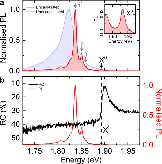
Photoluminescence and reflectance contrast spectra of hBN-encapsulated 1L-WSeS. (a) PL spectrum from the encapsulated 1L-WSe device (red curve) compared to the PL spectrum from unencapsulated 1L-WSeS (blue curve). The spectra are normalized to the same peak height. The peaks labeled 1, 2, and 3 are present across the device. The inset shows the magnified PL spectrum around X0. (b) RC spectrum (black curve, left axis) from the encapsulated 1L-WSe device compared to the PL spectrum at the same location (red curve, right axis). The black dashed line denotes the X0 transition energy, 1.893 eV. All spectra were acquired at 4 K, in the neutral-doping regime, and the PL spectra under 2.33 eV excitation.
The peaks labeled 1, 2, 3, and X0 are present in the 1L-WSeS PL spectra across the whole device (see S3), indicating that these arise from intrinsic excitonic transitions. Since the highest-energy PL peak in both 1L-WSe2 and 1L-WS2 stems from neutral excitons,42 the peak at 1.893 eV is a likely candidate for the neutral exciton, X0, in 1L-WSe. To verify this, we directly probe excitonic absorption resonances using RC spectroscopy (see Methods).14
Figure 2b shows a RC spectrum from our 1L-WSeS device (black curve) and the PL spectrum from the same location (red curve). The RC signal shows a strong feature at 1.893 eV, which confirms our assignment of X0. The lowest observed PL FWHM of the Janus X0 transition is 5.9 meV in our device, the lowest reported to date. The X0 transition is present in both PL and RC across the fully converted Janus region (see S3), with an average PL transition energy of 1.890(1) eV and an average FWHM of 8.4(4) meV over 11 measured locations.
Power-dependent PL measurements (see S4) provide further evidence that X0 is the neutral exciton transition as its intensity scales linearly with power over the measured range 15 nW to 50 μW (corresponding to 3 Wcm–2 to 104 Wcm–2). We note that in the spectral range 1.750 to 1.825 eV we also observe PL peaks with linear power dependences at low power and that saturate in the range 50 to 500 nW (10 to 100 Wcm–2). This suggests the presence of localized defects displaying quantum light emission.20,47,48
Density functional theory (DFT) calculations of the 1L-WSeS band structure (see S5) show that, similar to conventional W-based TMDs (1L-WSe2 and 1L-WS2),49−51 1L-WSe is direct-bandgap at the K points, with a spin ordering such that the upper valence band is opposite in spin to the lower spin-split conduction band. The spin ordering in the conduction band allows for both a negatively charged intervalley trion (Xinter–), with the two electrons in different valleys, and an intravalley trion (Xintra), with the two electrons in the same valley. By combining DFT and quantum Monte Carlo calculations we predict the binding energies of the Coulomb-exchange split Xinter– and Xintra to be 26 and 32 meV, respectively, relative to the neutral exciton in free-standing 1L-WSeS.
Voltage-Controlled Generation of Charged Excitons
To measure the charged excitonic transitions of 1L-WSeS, we tune its doping by applying a voltage V between the 1L-WSe and the Si substrate. Figure 3a shows the RC derivative signal as we vary the doping density, n (Methods). Similar doping dependence is observed on a second device (see S2). In the operational range of voltages, only the n-doped regime is accessible, due to an intrinsic n-doping ∼3 × 1012 cm–2. The previously identified X0 transition, here at 1.896 eV, dominates the RC signal between +21 to +17 V, corresponding to charge neutrality. As we decrease the voltage, and n-dope the 1L-WSeS, lower energy transitions appear, which are analogous to the transitions observed in the n-doped regime for 1L-WSe2.52−54
Figure 3.

Charge dependence of the reflectance contrast spectrum of 1L-WSeS. (a) RC derivative with varying electron doping density n (left axis) and applied voltage (right axis) at 4 K. (b) RC derivative spectra at the voltages corresponding to the dashed white linecuts in panel (a) at 19, 7, and −10 V. The excitonic transitions X0, Xinter, Xintra–, and X–′ are labeled.
Figure 3b presents the RC derivative at 19, 7, and −10 V. The neutral exciton, X0, is shown in the line cut at 19 V. Between +17 to +5 V, we see a doublet, which we identify as Xinter– and Xintra in the line cut at 7 V with peaks at 1.864 and 1.857 eV. We find an average binding energy relative to X0 of 33.4(5) meV and 39.9(3) meV for Xinter– and Xintra, respectively, over seven measured locations. We attribute the difference in binding energies of these trions compared to our calculations to a difference in dielectric environment caused by ML-hBN encapsulation.55 The exchange splitting between the negative trion transitions of 6.4(6) meV is in good agreement with our calculations.
At increased n-doping, below 5 V, the Xinter– and Xintra peaks vanish and a single peak, labeled X–′ in the linecut at −10 V in Figure 3b, dominates the derivative of the RC spectrum. The X–′ peak initially appears at 1.845 eV and redshifts by 10 meV between +5 and −17 V. An excitonic transition with a similar doping dependence has previously been observed in 1L-WSe253,54,56 and attributed to excitons bound to intervalley plasmons.56,57 We expect this peak in 1L-WSeS to be similar in origin, due to the similarity in its behavior with the transition observed in 1L-WSe2.
Magnetic-Field Dependence of Janus Excitons
We next probe the exciton g factors by applying an out-of-plane magnetic field, B, and measuring the Zeeman energy splitting of the exciton transitions. We send unpolarized light to the device and detect the RC spectra with both σ+ and σ– circular polarizations. The left-aligned panels (a, c, e, and g) in Figure 4 display the RC derivative spectra for each excitonic transition measured at B = 3 T magnetic field, with the right-circular (σ+) and left-circular (σ–) polarizations shown by the blue and red curves, respectively. The splitting ΔE as a function of B is shown in the right-hand panels (b, d, f, and h) of Figure 4. Linear fits give the magnitude of the exciton transition g factors, where ΔE = −gμBB (μB = 58 μeV T–1 is the Bohr magneton).
Figure 4.

Magnetic field dependence of the excitonic complexes in 1L-WSeS. (a) RC derivative spectrum with σ+ (blue) and σ– (red) polarized collection at B = 3 T for X0 (at 19 V). (b) The energy splitting ΔE between X0 peaks in σ+ and σ– detected light as a function of magnetic field. The left panel shows the average splitting measured with RC in the neutral regime (splitting averaged between 18 to 20 V at each magnetic field). The right panel shows the splitting of X0 measured with PL. The solid curve is a linear fit to ΔE = −gμBB, and the g factors are displayed for both RC and PL. (c) Same measurement as in (a) but for Xinter at 12.5 V. (d) ΔE as a function of magnetic field for Xinter– at 12.5 V. (e,f) Same as in (c) and (d) but for Xintra at 9 V. (g,h) Same as in (c) and (d) but for the X–′ peak at −20 V. All measurements were carried out at 4 K.
Figure 4a presents the RC derivative spectra for X0 at 3 T, showing a well-resolved splitting. Figure 4b shows ΔE for X0 as a function of magnetic field, for both RC and PL. From the linear fit we extract similar g factors of 4.5(2) and 4.14(6) for RC and PL, respectively. For conventional 1L-TMDs, g factors ∼4 have typically been assigned to bright excitons in the K and K′ valleys, with valley, orbital, and spin contributing to the magnetic moment.58,59 The measured g factors are consistent with 1L-WSeS having a direct-bandgap at the K points.
The g factors of the negatively charged trions depend strongly on doping, ranging from 3 to 13 for voltages from 8 to 14 V (see S6). For conventional 1L-TMDs, a similar dependence and resulting trion g factors greater than 4 have been attributed to many-body interactions with the Fermi sea of electrons.60,61 We expect a similar origin of the observed doping-dependent trion g factor in 1L-WSeS. Figure 4c–f shows RC derivative spectra and splittings as a function of magnetic field for the negative trions at example voltages. We find example g factors of 5.7(7) for Xinter and 5.4(6) for Xintra– at the voltages presented. The Xinter and Xintra– transitions additionally show evidence of the thermalization of the excess charge, as observed in conventional W-based 1L-TMDs.45,59,62 Beyond ∼3 T, this leads to only a single polarization being observable for each negative trion.
Figure 4g shows the polarization-resolved RC derivative spectrum for the X–′ transition at 3 T. Figure 4h displays the RC splitting of X–′ as a function of magnetic field, which gives a g factor ∼ 4.1(4), consistent with the interpretation of X–′ as the exciton bound to intervalley plasmons and dressed by many-body interactions.53,54,56
Conclusions
We identified several excitonic complexes in Janus 1L-WSeS: X0, Xinter, Xintra–, and X–′ and measured their g factors by integrating a hBN encapsulated 1L-WSe into a charge-control device. Integrating J-TMDs into vertical heterostructures is key for the future development of nanoscale optoelectronic devices,63,64 while resolving few-meV exciton line widths and identifying the exciton spectrum determines the suitability of J-TMDs for sensing.65,66 Future work includes identifying the transitions that give rise to the as-yet unidentified PL peaks as well as measuring the excitonic spectrum in the positively doped regime. An immediate next step is measuring the out-of-plane electric dipole moment of excitons in 1L-WSeS by applying an out-of-plane electric field in a capacitor-like device structure. The predicted permanent electric dipole moment of ∼0.2 D for the Janus X031,67 means that the resulting Stark shift ∼4 meV at 1 V/nm would be resolved with our ∼6 meV line widths.
Methods
Fabrication
We build our device by following a multistep process: first, the bottom ML-hBN is mechanically exfoliated onto a Si/SiO2 (90 nm oxide thickness) substrate. Second, a parent 1L-WSe2 is mechanically exfoliated from a flux-zone grown68 bulk WSe2 crystal and deposited on the bottom ML-hBN by polydimethylsiloxane (PDMS) transfer. Third, the 1L-WSe2 undergoes AFM flattening69 and subsequent conversion to a Janus 1L-WSeS by using the selective epitaxial atomic replacement (SEAR) method,36 while recording time-resolved Raman spectroscopy measurements in-situ to achieve deterministic conversion.37 Fourth, the top ML-hBN and FLG are sequentially deposited on the 1L-WSe by PDMS transfer, with annealing to 150 °C and AFM flattening after each layer is deposited. The FLG is mechanically exfoliated from graphite sourced from HQ Graphene. Fifth, Au contacts are deposited using standard electron-beam lithography procedures.
AFM topography (Bruker Icon) is used to confirm the layer thicknesses, and Raman spectroscopy (Horiba LabRam Evolution) is used to characterize the various constituents of the heterostructure, along with confirming the conversion from 1L-WSe2 to 1L-WSeS (see S1).
Optical Measurements
All 4 K measurements are taken in a closed-cycle cryostat (AttoDRY 1000 from Attocube Systems AG), equipped with an 8 T superconducting magnet.
Excitation and collection light pass through a home-built confocal microscope in reflection geometry, with a 0.81 numerical aperture (NA) apochromatic objective (LT-APO/NIR/0.81 from Attocube Systems AG). The PL measurements use continuous-wave excitation from a 2.33 eV laser (Ventus 532 from Laser Quantum Ltd.), with the excitation powers measured on the sample and the optical intensity calculated from the optical spot size given by the 0.81 NA. The PL signal is sent to a 150-line grating spectrometer (Princeton Instruments Inc.).
The RC measurements use broadband light (Thorlabs mounted LED M660L4, nominal wavelength 660 nm, FWHM 20 nm). The reflected light is collected in the confocal microscope discussed above and the spectra are recorded on the same 150-line grating spectrometer as for PL. RC is calculated by comparing the spectrum reflected from the heterostructure in a region with the 1L-WSeS, R, and without 1L-WSe, R0. RC as a function of emission energy E is then given by
The negative derivative of the RC spectrum, −d(RC)/dE, highlights the excitonic transitions and suppresses the RC background.53,70,71 To obtain the derivative RC spectrum, we first smooth the raw RC spectrum using a spline fit and then take the derivative of the resultant spline.
Gate-Voltage to Layer-Doping Conversion
The doping density n (charge per unit area) is calculated from the applied voltage V (Keithley 2400 SMU), by using the gate capacitance, C
The intrinsic doping, ni, is the doping density at zero applied voltage, and the magnitude of the electron charge is qe = 1.6 × 10⁻¹⁹ C.
The voltage is applied across both the ML-hBN and SiO2 and the gate capacitance can be derived by combining the dielectric layers of ML-hBN and SiO2 in series
The relative dielectric constants of SiO2 and hBN are ϵSiO2 = 3.972 and ϵhBN = 3.8,73 respectively. ϵ0 = 8.85 × 10¹² Fm–1 is the vacuum permittivity.
The thickness of SiO2 is dSiO2 = 90 nm and that of hBN is dhBN = 27 nm (see S1). The intrinsic doping density is ni = 3 × 1012 cm–2, determined by setting the doping density to n = 0 when the reflectance contrast signal from the neutral exciton vanishes (17 V),53 where positive n indicates electron doping.
Acknowledgments
We acknowledge funding from the EU Quantum Technology (2D-SIPC) and Graphene Flagships; EU Grants CHARM and Graph-X; ERC Grants PEGASOS, Hetero2D, GSYNCOR, and GIPT; and EPSRC Grants EP/K01711X/1, EP/K017144/1, EP/N010345/1, EP/L016087/1, EP/X015742/1, and EP/V000055/1. M.S.G.F. acknowledges the EPSRC Doctoral Training Programme. D.M.K. acknowledges support of a Royal Society university research fellowship URF\R1\180593. S.T. acknowledges primary support from DOE-SC0020653 (materials synthesis), NSF CMMI 1825594 (NMR and TEM studies), NSF DMR-2206987 (magnetic measurements), NSF CMMI-1933214, NSF 1904716, NSF 1935994, NSF ECCS 2052527, DMR 2111812, and CMMI 2129412 (scalability of Janus layers). K.W. and T.T. acknowledge support from the JSPS KAKENHI (Grant Numbers 19H05790, 20H00354 and 21H05233).
Supporting Information Available
The Supporting Information is available free of charge at https://pubs.acs.org/doi/10.1021/acsnano.2c10697.
Device characterization; Gate-dependent measurements in device 2; Spectral mapping and homogeneity; Power-dependent measurements; Band structure calculations; Magnetic-field dependent measurements (PDF)
Author Contributions
# M.S.G.F., A.R.-P.M., and M.Y.S. contributed equally to this work.
Author Contributions
A.R.-P.M., M.S.G.F., A.C.F., D.M.K., and M.A. conceived and managed the project; M.Y.S., Y.Q., P.K., J.K., and S.T. provided the bulk WSe2 crystals and carried out the Janus SEAR conversion; K.W. and T.T. provided hBN crystals; A.R.C., B.L.T.R., and J.K. fabricated the devices; E.M. performed the calculations; M.S.G.F., A.R.-P.M., C.M.P., E.M.A., R.K., D.M.K., and M.A. performed the optical measurements and analyzed the results. All authors participated in the discussion of the results and the writing of the manuscript.
The authors declare no competing financial interest.
Notes
This work has previously been submitted to a preprint server:74 Feuer, M. S. G.; Montblanch, A. R. P.; Sayyad, M.; Purser, C. M.; Qin, Y.; Alexeev, E. M.; Cadore, A. R.; Rosa, B. L. T.; Kerfoot, J.; Mostaani, E.; Kalba, R.; Kolari, P.; Kopaczek, J.; Watanabe, K.; Taniguchi, T.; Ferrari, A. C.; Kara, D. M.; Tongay, S.; Atature, M. Identification of exciton complexes in a charge-tunable Janus WSeS monolayer. arXiv, October 13, 2022, arXiv:2210.06930. DOI: 10.48550/arXiv.2210.06930 (accessed March 22, 2023).
Supplementary Material
References
- Novoselov K. S.; Jiang D.; Schedin F.; Booth T.; Khotkevich V.; Morozov S.; Geim A. K. Two-dimensional atomic crystals. Proc. Natl. Acad. Sci. U. S. A. 2005, 102, 10451–10453. 10.1073/pnas.0502848102. [DOI] [PMC free article] [PubMed] [Google Scholar]
- Radisavljevic B.; Radenovic A.; Brivio J.; Giacometti V.; Kis A. Single-layer MoS2 transistors. Nat. Nanotechnol. 2011, 6, 147–150. 10.1038/nnano.2010.279. [DOI] [PubMed] [Google Scholar]
- Palacios-Berraquero C.; Kara D. M.; Montblanch A. R.-P.; Barbone M.; Latawiec P.; Yoon D.; Ott A. K.; Loncar M.; Ferrari A. C.; Atatüre M. Large-scale quantum-emitter arrays in atomically thin semiconductors. Nat. Commun. 2017, 8, 1–6. 10.1038/ncomms15093. [DOI] [PMC free article] [PubMed] [Google Scholar]
- Ferrari A. C.; Bonaccorso F.; Fal’ko V.; Novoselov K. S.; Roche S.; Bøggild P.; Borini S.; Koppens F. H. L.; Palermo V.; Pugno N.; Garrido J. A.; Sordan R.; Bianco A.; Ballerini L.; Prato M.; Lidorikis E.; Kivioja J.; Marinelli C.; Ryhänen T.; Morpurgo A.; et al. Science and technology roadmap for graphene, related two-dimensional crystals, and hybrid systems. Nanoscale 2015, 7, 4598–4810. 10.1039/C4NR01600A. [DOI] [PubMed] [Google Scholar]
- Koppens F.; Mueller T.; Avouris P.; Ferrari A.; Vitiello M.; Polini M. Photodetectors based on graphene, other two-dimensional materials and hybrid systems. Nat. Nanotechnol. 2014, 9, 780–793. 10.1038/nnano.2014.215. [DOI] [PubMed] [Google Scholar]
- Kou L.; Ma Y.; Sun Z.; Heine T.; Chen C. Two-dimensional topological insulators: Progress and prospects. J. Phys. Chem. Lett. 2017, 8, 1905–1919. 10.1021/acs.jpclett.7b00222. [DOI] [PubMed] [Google Scholar]
- Bonaccorso F.; Lombardo A.; Hasan T.; Sun Z.; Colombo L.; Ferrari A. C. Production and processing of graphene and 2d crystals. Mater. Today 2012, 15, 564–589. 10.1016/S1369-7021(13)70014-2. [DOI] [Google Scholar]
- Geim A. K.; Grigorieva I. V. Van der Waals heterostructures. Nature 2013, 499, 419–425. 10.1038/nature12385. [DOI] [PubMed] [Google Scholar]
- Backes C.; Abdelkader A. M.; Alonso C.; Andrieux A.; Arenal R.; Azpeitia J.; Balakrishnan N.; Banszerus L.; Barjon J.; Bartali R.; Bellani S.; Berger C.; Berger R.; Bernal Ortega M. M.; Bernard C.; Beton P. H.; Beyer A.; Bianco A.; Bøggild P.; Bonaccorso F.; et al. Production and processing of graphene and related materials. 2D Mater. 2020, 7, 022001. 10.1088/2053-1583/ab1e0a. [DOI] [Google Scholar]
- Mak K. F.; Lee C.; Hone J.; Shan J.; Heinz T. F. Atomically thin MoS2: a new direct-gap semiconductor. Phys. Rev. Lett. 2010, 105, 136805. 10.1103/PhysRevLett.105.136805. [DOI] [PubMed] [Google Scholar]
- Xiao D.; Liu G.-B.; Feng W.; Xu X.; Yao W. Coupled spin and valley physics in monolayers of MoS2 and other group-VI dichalcogenides. Phys. Rev. Lett. 2012, 108, 196802. 10.1103/PhysRevLett.108.196802. [DOI] [PubMed] [Google Scholar]
- Jones A. M.; Yu H.; Ghimire N. J.; Wu S.; Aivazian G.; Ross J. S.; Zhao B.; Yan J.; Mandrus D. G.; Xiao D.; Yao W.; Xu X. Optical generation of excitonic valley coherence in monolayer WSe2. Nat. Nanotechnol. 2013, 8, 634–638. 10.1038/nnano.2013.151. [DOI] [PubMed] [Google Scholar]
- Zeng H.; Dai J.; Yao W.; Xiao D.; Cui X. Valley polarization in MoS2 monolayers by optical pumping. Nat. Nanotechnol. 2012, 7, 490–493. 10.1038/nnano.2012.95. [DOI] [PubMed] [Google Scholar]
- Mak K. F.; He K.; Shan J.; Heinz T. F. Control of valley polarization in monolayer MoS2 by optical helicity. Nat. Nanotechnol. 2012, 7, 494–498. 10.1038/nnano.2012.96. [DOI] [PubMed] [Google Scholar]
- Wang G.; Chernikov A.; Glazov M. M.; Heinz T. F.; Marie X.; Amand T.; Urbaszek B. Colloquium: Excitons in atomically thin transition metal dichalcogenides. Rev. Mod. Phys. 2018, 90, 021001. 10.1103/RevModPhys.90.021001. [DOI] [Google Scholar]
- Kang J.; Tongay S.; Zhou J.; Li J.; Wu J. Band offsets and heterostructures of two-dimensional semiconductors. Appl. Phys. Lett. 2013, 102, 012111. 10.1063/1.4774090. [DOI] [Google Scholar]
- Gong C.; Zhang H.; Wang W.; Colombo L.; Wallace R. M.; Cho K. Band alignment of two-dimensional transition metal dichalcogenides: Application in tunnel field effect transistors. Appl. Phys. Lett. 2013, 103, 053513. 10.1063/1.4817409. [DOI] [Google Scholar]
- Mak K. F.; Shan J. Opportunities and challenges of interlayer exciton control and manipulation. Nat. Nanotechnol. 2018, 13, 974–976. 10.1038/s41565-018-0301-1. [DOI] [PubMed] [Google Scholar]
- Jauregui L. A.; Joe A. Y.; Pistunova K.; Wild D. S.; High A. A.; Zhou Y.; Scuri G.; De Greve K.; Sushko A.; Yu C.-H.; Taniguchi T.; Watanabe K.; Needleman D. J.; Lukin M. D.; Park H.; Kim P. Electrical control of interlayer exciton dynamics in atomically thin heterostructures. Science 2019, 366, 870–875. 10.1126/science.aaw4194. [DOI] [PubMed] [Google Scholar]
- Montblanch A. R.-P.; Kara D. M.; Paradisanos I.; Purser C. M.; Feuer M. S. G.; Alexeev E. M.; Stefan L.; Qin Y.; Blei M.; Wang G.; Cadore A. R.; Latawiec P.; Loncar M.; Tongay S.; Ferrari A. C.; Atatüre M. Confinement of long-lived interlayer excitons in WS2/WSe2 heterostructures. Commun. Phys. 2021, 4, 119. 10.1038/s42005-021-00625-0. [DOI] [Google Scholar]
- Jiang Y.; Chen S.; Zheng W.; Zheng B.; Pan A. Interlayer exciton formation, relaxation, and transport in TMD van der Waals heterostructures. Light Sci. Appl. 2021, 10, 1–29. 10.1038/s41377-021-00500-1. [DOI] [PMC free article] [PubMed] [Google Scholar]
- Huang D.; Choi J.; Shih C.-K.; Li X. Excitons in semiconductor moiré superlattices. Nat. Nanotechnol. 2022, 17, 227–238. 10.1038/s41565-021-01068-y. [DOI] [PubMed] [Google Scholar]
- Shabani S.; Halbertal D.; Wu W.; Chen M.; Liu S.; Hone J.; Yao W.; Basov D. N.; Zhu X.; Pasupathy A. N. Deep moiré potentials in twisted transition metal dichalcogenide bilayers. Nat. Phys. 2021, 17, 720–725. 10.1038/s41567-021-01174-7. [DOI] [Google Scholar]
- Andrei E. Y.; Efetov D. K.; Jarillo-Herrero P.; MacDonald A. H.; Mak K. F.; Senthil T.; Tutuc E.; Yazdani A.; Young A. F. The marvels of moiré materials. Nat. Rev. Mater. 2021, 6, 201–206. 10.1038/s41578-021-00284-1. [DOI] [Google Scholar]
- Cheng Y.; Zhu Z.; Tahir M.; Schwingenschlögl U. Spin-orbit-induced spin splittings in polar transition metal dichalcogenide monolayers. Europhys. Lett. 2013, 102, 57001. 10.1209/0295-5075/102/57001. [DOI] [Google Scholar]
- Yao Q.-F.; Cai J.; Tong W.-Y.; Gong S.-J.; Wang J.-Q.; Wan X.; Duan C.-G.; Chu J. Manipulation of the large Rashba spin splitting in polar two-dimensional transition-metal dichalcogenides. Phys. Rev. B 2017, 95, 165401. 10.1103/PhysRevB.95.165401. [DOI] [Google Scholar]
- Hu T.; Jia F.; Zhao G.; Wu J.; Stroppa A.; Ren W. Intrinsic and anisotropic Rashba spin splitting in Janus transition-metal dichalcogenide monolayers. Phys. Rev. B 2018, 97, 235404. 10.1103/PhysRevB.97.235404. [DOI] [Google Scholar]
- Dong L.; Lou J.; Shenoy V. B. Large in-plane and vertical piezoelectricity in Janus transition metal dichalchogenides. ACS Nano 2017, 11, 8242–8248. 10.1021/acsnano.7b03313. [DOI] [PubMed] [Google Scholar]
- Cui C.; Xue F.; Hu W.-J.; Li L.-J. Two-dimensional materials with piezoelectric and ferroelectric functionalities. npj 2D Mater. Appl. 2018, 2, 18. 10.1038/s41699-018-0063-5. [DOI] [Google Scholar]
- Jin H.; Wang T.; Gong Z.-R.; Long C.; Dai Y. Prediction of an extremely long exciton lifetime in a Janus-MoSTe monolayer. Nanoscale 2018, 10, 19310–19315. 10.1039/C8NR04568B. [DOI] [PubMed] [Google Scholar]
- Li F.; Wei W.; Zhao P.; Huang B.; Dai Y. Electronic and Optical Properties of Pristine and Vertical and Lateral Heterostructures of Janus MoSSe and WSSe. J. Phys. Chem. Lett. 2017, 8, 5959–5965. 10.1021/acs.jpclett.7b02841. [DOI] [PubMed] [Google Scholar]
- Zheng T.; Lin Y.-C.; Yu Y.; Valencia-Acuna P.; Puretzky A. A.; Torsi R.; Liu C.; Ivanov I. N.; Duscher G.; Geohegan D. B.; Ni Z.; Xiao K.; Zhao H. Excitonic Dynamics in Janus MoSSe and WSSe Monolayers. Nano Lett. 2021, 21, 931–937. 10.1021/acs.nanolett.0c03412. [DOI] [PubMed] [Google Scholar]
- Zhang J.; Jia S.; Kholmanov I.; Dong L.; Er D.; Chen W.; Guo H.; Jin Z.; Shenoy V. B.; Shi L.; Lou J. Janus monolayer transition-metal dichalcogenides. ACS Nano 2017, 11, 8192–8198. 10.1021/acsnano.7b03186. [DOI] [PubMed] [Google Scholar]
- Lu A.-Y.; Zhu H.; Xiao J.; Chuu C.-P.; Han Y.; Chiu M.-H.; Cheng C.-C.; Yang C.-W.; Wei K.-H.; Yang Y.; Wang Y.; Sokaras D.; Nordlund D.; Yang P.; Muller D. A.; Chou M.-Y.; Zhang X.; Li L.-J. Janus monolayers of transition metal dichalcogenides. Nat. Nanotechnol. 2017, 12, 744–749. 10.1038/nnano.2017.100. [DOI] [PubMed] [Google Scholar]
- Gan Z.; Paradisanos I.; Estrada-Real A.; Picker J.; Najafidehaghani E.; Davies F.; Neumann C.; Robert C.; Wiecha P.; Watanabe K.; Taniguchi T.; Marie X.; Biskupek J.; Mundszinger M.; Leiter R.; Kaiser U.; Krasheninnikov A. V.; Urbaszek B.; George A.; Turchanin A. Chemical vapor deposition of high optical quality large area monolayer Janus transition metal dichalcogenides. Adv. Mater. 2022, 34, 2205226. 10.1002/adma.202205226. [DOI] [PubMed] [Google Scholar]
- Zhang X.; Lou F.; Li C.; Zhang X.; Jia N.; Yu T.; He J.; Zhang B.; Xia H.; Wang S.; Tao X. Flux method growth of bulk MoS2 single crystals and their application as a saturable absorber. CrystEngComm 2015, 17, 4026–4032. 10.1039/C5CE00484E. [DOI] [Google Scholar]
- Trivedi D. B.; Turgut G.; Qin Y.; Sayyad M. Y.; Hajra D.; Howell M.; Liu L.; Yang S.; Patoary N. H.; Li H.; Petric M. M.; Meyer M.; Kremser M.; Barbone M.; Soavi G.; Stier A. V.; Müller K.; Yang S.; Esqueda I. S.; Zhuang H.; et al. Room-Temperature Synthesis of 2D Janus Crystals and their Heterostructures. Adv. Mater. 2020, 32, 2006320. 10.1002/adma.202006320. [DOI] [PubMed] [Google Scholar]
- Qin Y.; Sayyad M.; Montblanch A. R.-P.; Feuer M. S. G.; Dey D.; Blei M.; Sailus R.; Kara D. M.; Shen Y.; Yang S.; Botana A. S.; Atatüre M.; Tongay S. Reaching the Excitonic Limit in 2D Janus Monolayers by In Situ Deterministic Growth. Adv. Mater. 2022, 34, 2106222. 10.1002/adma.202106222. [DOI] [PubMed] [Google Scholar]
- Tonndorf P.; Schmidt R.; Böttger P.; Zhang X.; Börner J.; Liebig A.; Albrecht M.; Kloc C.; Gordan O.; Zahn D. R. T.; Michaelis de Vasconcellos S.; Bratschitsch R. Photoluminescence emission and Raman response of monolayer MoS2, MoSe2, and WSe2. Opt. Express 2013, 21, 4908–4916. 10.1364/OE.21.004908. [DOI] [PubMed] [Google Scholar]
- Petrić M. M.; Kremser M.; Barbone M.; Qin Y.; Sayyad Y.; Shen Y.; Tongay S.; Finley J. J.; Botello-Méndez A. R.; Müller K. Raman spectrum of Janus transition metal dichalcogenide monolayers WSSe and MoSSe. Phys. Rev. B 2021, 103, 035414. 10.1103/PhysRevB.103.035414. [DOI] [Google Scholar]
- Duan X.; Wang C.; Fan Z.; Hao G.; Kou L.; Halim U.; Li H.; Wu X.; Wang Y.; Jiang J.; Pan A.; Huang Y.; Yu R.; Duan X. Synthesis of WS2xSe2–2x alloy nanosheets with composition-tunable electronic properties. Nano Lett. 2016, 16, 264–269. 10.1021/acs.nanolett.5b03662. [DOI] [PubMed] [Google Scholar]
- Yan T.; Qiao X.; Liu X.; Tan P.; Zhang X. Photoluminescence properties and exciton dynamics in monolayer WSe2. Appl. Phys. Lett. 2014, 105, 101901. 10.1063/1.4895471. [DOI] [Google Scholar]
- Cadiz F.; Courtade E.; Robert C.; Wang G.; Shen Y.; Cai H.; Taniguchi T.; Watanabe K.; Carrere H.; Lagarde D.; Manca M.; Amand T.; Renucci P.; Tongay S.; Marie X.; Urbaszek B. Excitonic Linewidth Approaching the Homogeneous Limit in MoS2-Based van der Waals Heterostructures. Physical Review X 2017, 7, 021026. 10.1103/PhysRevX.7.021026. [DOI] [Google Scholar]
- Dean C. R.; Young A. F.; Meric I.; Lee C.; Wang L.; Sorgenfrei S.; Watanabe K.; Taniguchi T.; Kim P.; Shepard K. L.; Hone J. Boron nitride substrates for high-quality graphene electronics. Nat. Nanotechnol. 2010, 5, 722–726. 10.1038/nnano.2010.172. [DOI] [PubMed] [Google Scholar]
- Man M. K.; Deckoff-Jones S.; Winchester A.; Shi G.; Gupta G.; Mohite A. D.; Kar S.; Kioupakis E.; Talapatra S.; Dani K. M. Protecting the properties of monolayer MoS2 on silicon based substrates with an atomically thin buffer. Sci. Rep. 2016, 6, 1–9. 10.1038/srep20890. [DOI] [PMC free article] [PubMed] [Google Scholar]
- Barbone M.; Montblanch A. R.-P.; Kara D. M.; Palacios-Berraquero C.; Cadore A. R.; De Fazio D.; Pingault B.; Mostaani E.; Li H.; Chen B.; Watanabe K.; Taniguchi T.; Tongay S.; Wang G.; Ferrari A. C.; Atatüre M. Charge-tuneable biexciton complexes in monolayer WSe2. Nat. Commun. 2018, 9, 1–6. 10.1038/s41467-018-05632-4. [DOI] [PMC free article] [PubMed] [Google Scholar]
- Li Z.; Wang T.; Lu Z.; Jin C.; Chen Y.; Meng Y.; Lian Z.; Taniguchi T.; Watanabe K.; Zhang S.; Smirnov D.; Shi S.-F. Revealing the biexciton and trion-exciton complexes in BN encapsulated WSe2. Nat. Commun. 2018, 9, 1–7. 10.1038/s41467-018-05863-5. [DOI] [PMC free article] [PubMed] [Google Scholar]
- Kurtsiefer C.; Mayer S.; Zarda P.; Weinfurter H. Stable solid-state source of single photons. Phys. Rev. Lett. 2000, 85, 290. 10.1103/PhysRevLett.85.290. [DOI] [PubMed] [Google Scholar]
- He Y.-M.; Clark G.; Schaibley J. R.; He Y.; Chen M.-C.; Wei Y.-J.; Ding X.; Zhang Q.; Yao W.; Xu X.; Lu C.-Y.; Pan J.-W. Single quantum emitters in monolayer semiconductors. Nat. Nanotechnol. 2015, 10, 497–502. 10.1038/nnano.2015.75. [DOI] [PubMed] [Google Scholar]
- Liu G.-B.; Shan W.-Y.; Yao Y.; Yao W.; Xiao D. Three-band tight-binding model for monolayers of group-VIB transition metal dichalcogenides. Phys. Rev. B 2013, 88, 085433. 10.1103/PhysRevB.88.085433. [DOI] [Google Scholar]
- Kośmider K.; González J. W.; Fernández-Rossier J. Large spin splitting in the conduction band of transition metal dichalcogenide monolayers. Phys. Rev. B 2013, 88, 245436. 10.1103/PhysRevB.88.245436. [DOI] [Google Scholar]
- Kormányos A.; Burkard G.; Gmitra M.; Fabian J.; Zólyomi V.; Drummond N. D.; Fal’ko V. k·p theory for two-dimensional transition metal dichalcogenide semiconductors. 2D Materials 2015, 2, 022001. 10.1088/2053-1583/2/2/022001. [DOI] [Google Scholar]
- Courtade E.; Semina M.; Manca M.; Glazov M. M.; Robert C.; Cadiz F.; Wang G.; Taniguchi T.; Watanabe K.; Pierre M.; Escoffier W.; Ivchenko E. L.; Renucci P.; Marie X.; Amand T.; Urbaszek B. Charged excitons in monolayer WSe2: Experiment and theory. Phys. Rev. B 2017, 96, 085302. 10.1103/PhysRevB.96.085302. [DOI] [Google Scholar]
- Wang Z.; Zhao L.; Mak K. F.; Shan J. Probing the spin-polarized electronic band structure in monolayer transition metal dichalcogenides by optical spectroscopy. Nano Lett. 2017, 17, 740–746. 10.1021/acs.nanolett.6b03855. [DOI] [PubMed] [Google Scholar]
- Wang Z.; Shan J.; Mak K. F. Valley- and spin-polarized Landau levels in monolayer WSe2. Nat. Nanotechnol. 2017, 12, 144–149. 10.1038/nnano.2016.213. [DOI] [PubMed] [Google Scholar]
- Van Tuan D.; Yang M.; Dery H. Coulomb interaction in monolayer transition-metal dichalcogenides. Phys. Rev. B 2018, 98, 125308. 10.1103/PhysRevB.98.125308. [DOI] [Google Scholar]
- Van Tuan D.; Scharf B.; Wang Z.; Shan J.; Mak K. F.; Žutić I.; Dery H. Probing many-body interactions in monolayer transition-metal dichalcogenides. Phys. Rev. B 2019, 99, 085301. 10.1103/PhysRevB.99.085301. [DOI] [Google Scholar]
- Van Tuan D.; Scharf B.; Žutić I.; Dery H. Marrying excitons and plasmons in monolayer transition-metal dichalcogenides. Physical Review X 2017, 7, 041040. 10.1103/PhysRevX.7.041040. [DOI] [Google Scholar]
- Aivazian G.; Gong Z.; Jones A. M.; Chu R.-L.; Yan J.; Mandrus D. G.; Zhang C.; Cobden D.; Yao W.; Xu X. Magnetic control of valley pseudospin in monolayer WSe2. Nat. Phys. 2015, 11, 148–152. 10.1038/nphys3201. [DOI] [Google Scholar]
- Koperski M.; Molas M. R.; Arora A.; Nogajewski K.; Bartos M.; Wyzula J.; Vaclavkova D.; Kossacki P.; Potemski M. Orbital, spin and valley contributions to Zeeman splitting of excitonic resonances in MoSe2, WSe2 and WS2 Monolayers. 2D Materials 2019, 6, 015001. 10.1088/2053-1583/aae14b. [DOI] [Google Scholar]
- Klein J.; Hötger A.; Florian M.; Steinhoff A.; Delhomme A.; Taniguchi T.; Watanabe K.; Jahnke F.; Holleitner A. W.; Potemski M.; Faugeras C.; Finley J. J.; Stier A. V. Controlling exciton many-body states by the electric-field effect in monolayer MoS2. Phys. Rev. Res. 2021, 3, L022009. 10.1103/PhysRevResearch.3.L022009. [DOI] [Google Scholar]
- Lyons T. P.; Dufferwiel S.; Brooks M.; Withers F.; Taniguchi T.; Watanabe K.; Novoselov K.; Burkard G.; Tartakovskii A. I. The valley Zeeman effect in inter- and intra-valley trions in monolayer WSe2. Nat. Commun. 2019, 10, 1–8. 10.1038/s41467-019-10228-7. [DOI] [PMC free article] [PubMed] [Google Scholar]
- Kapuściński P.; Vaclavkova D.; Grzeszczyk M.; Slobodeniuk A. O.; Nogajewski K.; Bartos M.; Watanabe K.; Taniguchi T.; Faugeras C.; Babiński A.; Potemski M.; Molas M. R. Valley polarization of singlet and triplet trions in a WS2 monolayer in magnetic fields. Phys. Chem. Chem. Phys. 2020, 22, 19155–19161. 10.1039/D0CP02737E. [DOI] [PubMed] [Google Scholar]
- Liu X.; Gao P.; Hu W.; Yang J. Photogenerated-carrier separation and transfer in two-dimensional Janus transition metal dichalcogenides and graphene van der Waals sandwich heterojunction photovoltaic cells. J. Phys. Chem. Lett. 2020, 11, 4070–4079. 10.1021/acs.jpclett.0c00706. [DOI] [PubMed] [Google Scholar]
- Tang X.; Kou L. 2D Janus Transition Metal Dichalcogenides: Properties and Applications. physica status solidi (b) 2022, 259, 2100562. 10.1002/pssb.202100562. [DOI] [Google Scholar]
- Yin W.; Tan H.; Ding P.; Wen B.; Li X.-B.; Teobaldi G.; Liu L.-M. Recent advances in low-dimensional Janus materials: theoretical and simulation perspectives. Materials Advances 2021, 2, 7543–7558. 10.1039/D1MA00660F. [DOI] [Google Scholar]
- Zhang L.; Xia Y.; Li X.; Li L.; Fu X.; Cheng J.; Pan R. Janus two-dimensional transition metal dichalcogenides. J. Appl. Phys. 2022, 131, 230902. 10.1063/5.0095203. [DOI] [Google Scholar]
- Xia C.; Xiong W.; Du J.; Wang T.; Peng Y.; Li J. Universality of electronic characteristics and photocatalyst applications in the two-dimensional Janus transition metal dichalcogenides. Phys. Rev. B 2018, 98, 165424. 10.1103/PhysRevB.98.165424. [DOI] [Google Scholar]
- Rosenberger M. R.; Chuang H.-J.; McCreary K. M.; Hanbicki A. T.; Sivaram S. V.; Jonker B. T. Nano-“squeegee” for the creation of clean 2D material interfaces. ACS Appl. Mater. Interfaces 2018, 10, 10379–10387. 10.1021/acsami.8b01224. [DOI] [PubMed] [Google Scholar]
- Chernikov A.; Berkelbach T. C.; Hill H. M.; Rigosi A.; Li Y.; Aslan O. B.; Reichman D. R.; Hybertsen M. S.; Heinz T. F. Exciton binding energy and nonhydrogenic Rydberg series in monolayer WS2. Phys. Rev. Lett. 2014, 113, 076802. 10.1103/PhysRevLett.113.076802. [DOI] [PubMed] [Google Scholar]
- Glazov M. M.; Ivchenko E. L.; Wang G.; Amand T.; Marie X.; Urbaszek B.; Liu B. Spin and valley dynamics of excitons in transition metal dichalcogenide monolayers. physica status solidi (b) 2015, 252, 2349–2362. 10.1002/pssb.201552211. [DOI] [Google Scholar]
- Kingon A. I.; Maria J.-P.; Streiffer S. Alternative dielectrics to silicon dioxide for memory and logic devices. Nature 2000, 406, 1032–1038. 10.1038/35023243. [DOI] [PubMed] [Google Scholar]
- Laturia A.; Van de Put M. L.; Vandenberghe W. G. Dielectric properties of hexagonal boron nitride and transition metal dichalcogenides: from monolayer to bulk. npj 2D Mater. Appl. 2018, 2, 1–7. 10.1038/s41699-018-0050-x. [DOI] [Google Scholar]
- Feuer M. S. G.; Montblanch A. R. P.; Sayyad M.; Purser C. M.; Qin Y.; Alexeev E. M.; Cadore A. R.; Rosa B. L. T.; Kerfoot J.; Mostaani E.; Kaleba R.; Kolari P.; Kopaczek J.; Watanabe K.; Taniguchi T.; Ferrari A. C.; Kara D. M.; Tongay S.; Atatüre M.. Identification of exciton complexes in a charge-tuneable Janus WSeS monolayer. arXiv, October 13, 2022, arXiv:2210.06930. 10.48550/arXiv.2210.06930 (accessed March 22, 2023). [DOI] [PMC free article] [PubMed]
Associated Data
This section collects any data citations, data availability statements, or supplementary materials included in this article.