

Abstract
Single modality wireless power transfer has limited depth for mm-sized implants across air / tissue or skull / tissue interfaces because they either suffer from high loss in tissue (RF, Optical) or high reflection at the medium interface (Ultrasound (US)). This paper proposes an RF-US relay chip at the media interface avoiding the reflection at the boundary, and enabling efficient wireless powering to mm-sized deep implants across multiple media. The relay chip rectifies the incoming RF power through an 85.5% efficient RF inductive link (across air) using a multi-output regulating rectifier (MORR) with 81% power conversion efficiency (PCE) at 186 mW load, and transmits ultrasound using adiabatic power amplifiers (PAs) to the implant in order to minimize cascaded power loss. To adapt the US focus to implant movement or placement, beamforming was implemented using 6 channels of US PAs with 2-bit phase control (0, 90, 180, and 270°) and 3 different amplitudes (6–29, 4.5, and 1.8 V) from the MORR. The adiabatic PA contributes a 30–40% increase in efficiency over class-D and beamforming increases the efficiency by 251% at 2.5 cm over fixed focusing. The proof-of-concept powering system for a retinal implant, from an external PA on a pair of glasses to a hydrophone with 1.2 cm (air) + 2.9 cm (agar eyeball phantom in mineral oil) separation distance, had a power delivered to the load (PDL) of 946 μW. The 2.3 × 2 mm2 relay chip was fabricated in a 180 nm high-voltage (HV) BCD process.
Index Terms—: wireless power transfer, power relay, phased array, beamforming, retinal implant, IMD, ultrasonic power transfer, multi-output regulating rectifier, adiabatic power amplifier, inductive powering, in-depth powering
I. Introduction
Implantable medical devices (IMDs) are a promising approach for treating a variety of disorders including paralysis [1]–[3], stroke [3], epilepsy [4], and vision loss [5]–[7] due to their ability to interface with high specificity within tissue. Modern IMDs use wires and large, bulky batteries which can cause tissue damage and infection [8]–[10]. Recent research has been aimed to miniaturize IMDs and reduce power to alleviate these complications, which has enabled wireless powering solutions [11]–[16].
Wireless powering has a few distinct advantages for mm-sized IMDs. Compared to bulky battery solutions, the implant can be further miniaturized with small transducers. The longevity of the device can be extended since it is no longer limited by the battery life. Eliminating the wire mitigates risk of infections and also helps simplify the surgery [17].
Current wirelessly powered IMDs are either powered by RF, optical (light) or ultrasound (US). Each modality has its own advantages and disadvantages. Near-field RF has high efficiency when the transducer size is comparable to the separation distance and minimally interacts with tissue, making it good for shallow implants that are under layers of heterogeneous material such as neural implants [18], [19]. Optical has the potential for extreme miniaturization since the wavelength is extremely small and the receivers can be integrated on chip [20]. However, scattering in tissue limits the implant depth in most applications except the eye. Ultrasound has favorable properties including low loss propagation [21], [22], high allowed power intensity [23], and good transducer coupling due to mm wavelengths [14]. Because of these reasons, US has been used for powering IMDs for various sensing applications including blood pressure [24], ultrasound imaging [25], electrochemical sensing [26], [27], and neural recording [15], [28], [29]. However, it has high loss at the interface between air and tissue or bone and tissue [30].
Some implant applications require that the power be transferred across multiple media. When the difference in impedance between the various media becomes large, there is a significant loss at the interface due to reflections. For example, power must pass through the skull and then brain tissue for powering neural implants, and through the air and then the eye for retinal implants. For ultrasound, the difference in acoustic impedance for the above examples is large, resulting in almost all of the power being reflected [30]. This becomes critical when the wireless link must be efficient to supply power near the safety limits (few mWs). This is the case for future brain machine interfaces (BMIs) which seek to interact with the brain or retina with high resolution and large scale, and therefore the power must be high to maximize channel count [31], [32].
To pave the way for these future BMIs which have requirements of millimeter sized, cm depth across multiple media, and mWs of power, new wireless powering solutions are needed. Single modality solutions are limited: RF and optical cannot power at depth with high power and US has a large interface loss due to acoustic impedance mismatch across multiple media.
This paper is an extension of the work described in [33]. We expand on this work with additional circuit descriptions, analysis of the adiabatic power amplifier (PA) operation, and new measurements including XY plane acoustic beamforming and a new ex-vivo wireless power transmission experiment through a pig eye.
The paper is organized as follows. In Section II, we propose an RF-US relay system with beamforming capability to address the challenges of wirelessly powering deep implants across interfaces between different mediums and describe considerations for the RF inductive link, rectifier, and US link. Section III dives into detailed circuit descriptions and analysis of the rectifier, power management unit (PMU), and US PAs. The system performance is characterized in Section IV with measurements of the rectifier, US PAs, acoustic link, and full end-to-end wireless link. Finally, Section V concludes and compares the RF-US relay system to state of the art implant wireless powering systems.
II. Proposed System Architecture
Our proposed solution to power mm-sized implants at cm depth across multiple media is to utilize the strengths of both RF and US similar to [30]. A cm sized relay, shown in Fig. 1, is placed at the interface of the two media around 1 cm deep and converts incoming RF power to US power. The RF inductive link can transmit power efficiently across the cm air or skull layer, and the US can be focused to deep mm-sized implants in the tissue. The relay, which comprises of a receiver (Rx) coil, relay chip, and piezoelectric array, converts the received RF power to DC electrical power on the chip, and then converts the electrical power to ultrasound via PAs and the piezo array.
Fig. 1.

(a) RF-US relay adopted to a retinal implant powering application. (b) Conceptual image of the proposed RF-US relay system for wireless power transfer across the boundary of different media for deep mm-sized implants. The relay rectifies incoming RF energy and transmits US to wirelessly power the implant. (c) RF-US relay adopted to a deep brain implant application. (d) Simplified block diagram of the RF-US Relay and its associated cascaded power loss.
By converting RF to DC and then US instead of directly to US [30], we can control the amplitude and phase of each piezo element, fundamentally enabling dynamic control and programmability of the transmitted power in space through beamforming. Beamforming is critical for powering IMDs because the tissue can move, the implant can move within the tissue, or the surgical placement can be inaccurate.
In addition to assisting with beamforming, amplitude control enables power transmission control. For implants that are closer, farther away or require different power levels, the transmitted power needs to be adjusted accordingly. For this, multiple voltage supplies are needed. Specifically a dynamic high voltage supply is needed to cover the dynamic range of cm variation and power requirements ranging from μWs to mWs.
Although the relay architecture takes advantage of the strengths of RF and US, adding a relay inherently adds a cascaded power loss that must be minimized to avoid degrading the system efficiency to performance comparable to single modality solutions. The efficiency of each piece, shown in Fig. 1(d), is optimized in order to minimize this loss. The system efficiency is given by
| (1) |
| (2) |
where the power conversion efficiency (PCE) of the relay comprises of the rectification of the RF signal, voltage regulation, and conversion to ultrasound power.
In the following subsections, we will discuss the optimization and design decisions for the RF inductive link, multi-output regulating rectifier (MORR) that generates the multiple supply voltages, adiabatic PA, and US beamforming.
A. RF Inductive Link Design
The first piece of the system efficiency to optimize is the RF inductive link efficiency (ηRF–Inductive–Link). For wireless power transmission in air, RF powering is one of the most well established approaches among common modalities for providing high power density within a constrained specific absorption rate (SAR). Since the maximum geometrical parameters are already set by the application, the main design choice is the operation frequency. Considering the available frequency bands, we chose the 40.68 MHz power carrier frequency band in the industrial-scientific-medical band (ISM-band) as a trade-off between higher coil quality factors and rectifier switching loss. Lower frequency bands such as the 13.56 MHz band have lower coil quality factors and higher ISM bands such as 433.92 or 915 MHz degrade the PCE for AC-to-DC conversion at the rectifier due to higher switching loss, which is proportional to frequency [34].
The near-field RF inductive link is designed following the iterative design procedure in [35] with a consideration of existing interconnection to the coils in actual powering system implementation, and its electrical/geometrical parameters are summarized in Table I. In the high frequency structural simulator (HFSS) from ANSYS Inc. (Canonsburg, PA), the designed RF inductive link can achieve 86.6% simulated power transmission efficiency (PTE) with no eye rotation and 83.6% PTE with 15 degree eye rotation, which is likely to be the maximum angle between the Tx coil and Rx coil during the system operation (see Fig. 3). The maximum simulated specific absorption rate (SAR) averaged over 1 g of tissue across the HFSS eyeball model is 0.361 W/kg (see Fig. 4), which is below the FCC regulation, 1.6 W/kg, when the PDL is 186 mW.
TABLE I.
Electrical and geometrical parameters for the near-field RF inductive link design
| Geometrical / Electrical Parameters | Simulated Values |
|---|---|
| Tx coil (L1) | |
| Outer Diameter (D1) | 33 mm |
| Width (w1) / Spacing (s1) / Turns (N1) | 800 μm / 600 μm / 2 |
| Thickness (t1) | 35 μm (1 oz) |
| Inductance (L1) | 243 nH |
| Q-factor (Q1) | 104 |
| Rx coil (L2) | |
| Outer Diameter (D2) | 24 mm |
| Width (w2) / Spacing (s2) / Turns (N2) | 400 μm / 400 μm / 3 |
| Thickness (t2) | 35 μm (1 oz) |
| Inductance (L2) | 365 nH |
| Q-factor (Q2) | 99.8 |
| Load (RL / PL) | 537 Ω / 186 mW |
| Link | |
| Operating Frequency (f0) | 40.68 MHz |
| Coupling (k12) | 0.123 |
| Distance (d12) | 12 mm (air) |
| PTE | 86.6 % |
Fig. 3.
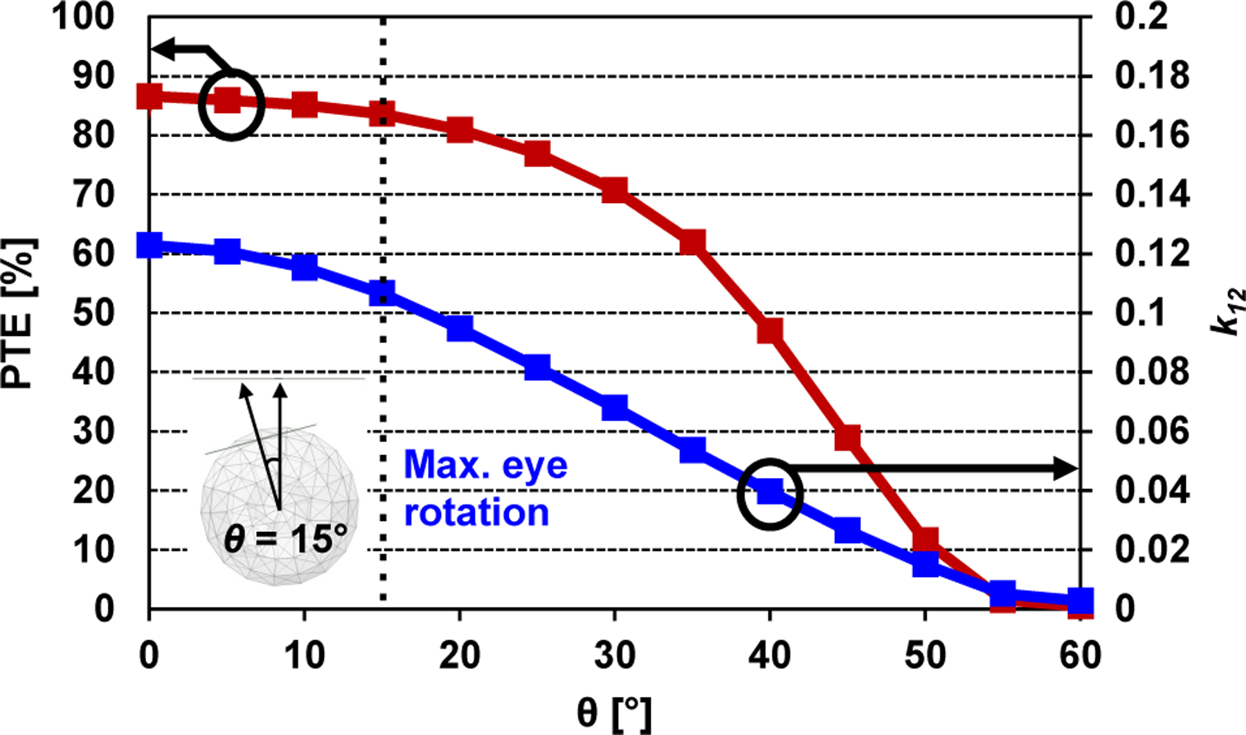
Simulated PTE (red) and coupling coefficient k12 (blue) of the RF inductive link versus eye rotation.
Fig. 4.

EM simulated SAR field averaged over a volume of 1 g of tissue for the HFSS eyeball model while delivering 186 mW to the load through the RF inductive link.
B. Overview of RF-US Relay Chip
The next piece of the system efficiency to maximize is the PCE (ηPCE) which occurs on the RF-US relay chip as shown in Fig. 1(d). The power conversion efficiency is made up of the rectifier efficiency (ηRect), regulation efficiency (ηReg), and the US PA efficiency (ηUS–PA). The chip is roughly divided into the power management unit (PMU) for AC-to-DC power conversion/voltage regulation (ηRect × ηReg) and 6-channel PAs (ηUS–PA) for US beamforming. Fig. 2 shows a detailed system diagram including a detailed breakdown of the main circuit blocks of the chip.
Fig. 2.

Detailed block diagram of the RF-US relay chip.
Two key designs are used to maximize the PCE. First the MORR generates and regulates the 3 supply voltages, needed for programmable amplitude and phase beamforming, including a high voltage (HV) supply in a single step to maximize ηRect × ηReg while avoiding additional cascaded power loss, as explained in Section III-A. Second, adiabatic low voltage (LV) PAs, discussed in Section III-C, can improve electrical-to-US PCE by recycling stored charges on parallel capacitors when driving capacitive piezo loads.
To accommodate high voltages, class-D HV PAs with an adjustable HV supply allow adjustment of power levels and the flexibility to drive different types of transducers such as piezos, piezoelectric micromachined ultrasonic transducers (PMUT), capacitive micromachined ultrasonic transducers (CMUT), and thin film piezos such as polyvinylidene fluoride (PVDF) and its composite variants. Overall the increased efficiency from the MORR and adiabatic PAs helps reduce the cascaded power loss and reduces the heating on the relay, allowing for higher transmit power.
C. US Link and Beamforming
The final piece of the system efficiency is the wireless power transmission from the relay to the implant ηUS–Link (see Fig. 1(d)). Ultrasound was selected for power transfer between the relay and implant due to low loss propagation (0.1 dB/cm/MHz in the vitreous [36], 0.5–1.0 dB/cm/MHz in tissue [21]), high transduction efficiency, beamforming/focusing capability [14] [37], and finally a high power safety limit of 7.2 mW/mm2 (tissue) and 0.5 mW/mm2 (eye) [23]. For example at 1 MHz the wavelength is around 1.5 mm, which we can match to the implant Rx for good transducer coupling and beamforming. Beamforming is critical in implant scenarios due to movement of the implant or tissue over time and variations in implant placement.
For application 1, the retina application (see Fig. 1(a)), the thickness of the piezo has to be less than the scleral contact lens thickness, which is typically less than <1 mm [38]. This means we either use the thickness mode at high frequency which requires many piezo elements or use a lower frequency with the area expansion mode [39]. For this proof of concept system, the area expansion mode is used to achieve a large transmit aperture with a small number of piezo elements.
For a given frequency, the US link is a function of Tx and Rx aperture size [40]. Given our transmit aperture size (12 × 12 mm2) and receive aperture (1.5 mm diameter), the simulated end-to-end US link focusing efficiency (ηUS–link) using the Field II ultrasound simulator at a depth of 2.5 cm [41], [42] was 2.18%. Compared to [30] which has an US PTE of 0.66% at 3 cm depth, this link has higher efficiency due to slightly smaller depth and larger Tx and Rx apertures. However, unlike [30] which has a fixed focus, the proposed US link will be programmable to enable dynamic, adaptive focusing. For comparison, a similar link using midfield RF powering across 1 cm of air and 4 cm of tissue to a 2 mm diameter implant achieves 0.04% efficiency [43].
III. Circuit Design and Considerations
A. MORR and Startup PMU
This section will first cover the architecture selection for the PMU, and then the implementation details of the MORR and startup PMU.
To maximize ηRect × ηReg and therefore the system efficiency, we must carefully select the architecture of the power management unit. Fig. 5 shows different possible architectures including conventional HV-compliance wireless power Rx generating multiple voltage supplies and our proposed MORR. The conventional structures shown in Fig. 5(a), (b), and (c) all have limitations either with voltage tunability, external component count, or cascaded power loss. The conventional power conversion structure with parallel rectifiers in Fig. 5(a) has more external capacitors for tuning the resonant frequency of the secondary coil, and less control on the absolute rectifier voltage outputs due to the fixed ratio of the multi-tapped inductor [44]. More common power conversion structures include a rectifier and DC-to-DC converters as shown in Fig. 5(b) and (c) [45]. The rectifier converts the received AC power across a Rx coil into DC power, and the DC-to-DC converter steps up/down the voltage. This 2-stage power conversion structure imposes cascaded power losses and results in a lower overall Rx PCE. To improve the limited PCE, direct resonant current- or voltage-mode battery charging [46], [47] and reconfigurable resonant regulating rectifiers [48], [49] were proposed. More recently, a dual LV output regulating rectifier [50] was proposed for applications which require different voltage supplies and output power depending on operation mode. However, these prior works are not suitable for IMDs which may require HV, typically over 10 V, and multiple different supplies. Examples include neural stimulators, implantable ultrasonic imagers with CMUTs, and RF-US power relay implants to power neural probes using ultrasound beamforming. To address the needs of the above applications, we designed a HV-compliance MORR and integrated it into the RF-US relay chip.
Fig. 5.

Conventional structures versus the proposed MORR.
Next, we will cover the circuit implementation and detailed operation of the MORR which generates and regulates 3 voltage supplies including a HV supply in a single step. Fig. 6 shows key operations of the MORR. There are 3 current paths for generating each of the supply voltages. The control of SW1–3 by the switching pulse generator determines which path the current from the coil flows into. For HV generation, the HV diode conducts when VIN>VHV and converts the incoming AC voltage into the DC HV (VHV <32 V) when SW1 is on. As shown in Fig. 6(a), the HV diode consists of two p-type 36 V laterally-diffused metal-oxide semiconductors (LDMOS) for current conduction and a Vth cancellation circuit to improve the PCE by reducing the voltage drop [51]. The DC HV is controlled by carefully tuning the output power of the external transmitter.
Fig. 6.

Operation modes of MORR for the high voltage, 4.7 V, and 2 V rectifier output paths.
The startup operation is as follows. The HV input bandgap reference (BGR) and the 4.5V / 1.8V HV input linear regulators start operating with the HV supply that is generated from the HV rectifier. The startup (SU) power-on-reset (POR) voltage, VSU_POR, becomes high with ~200 μs delay after the 1.8V HV input linear regulator output (VSU18) becomes stable. Next, the switching pulse generator for the LV regulating rectifiers starts operating with enabled VSU_POR.
For the operation of the two LV paths, the pulse delay modulation (PDM) switching pulse generator controls the half period switching timing to ensure that there is no reverse leakage current through SW1–3. When SW1 is off, the stored current (iL2) in the L2C2 tank charges CLV1 or CLV2. During this phase, VCP instantly changes from 0 to either VLV1 or VLV2, same as the in-phase current mode of the work with commercial-off-the-shelf (COTs) components in [52]. When VLV1 and VLV2 reach the target regulating voltages (4.7 V / 2 V), switching pulses are skipped for voltage regulation. Pulse skipping modulation (PSM) was adopted since switching losses for SW1–3 dominate conduction losses for light loads at high switching frequency [34], [53].
Fig. 7 shows the detailed schematic diagram of the switching pulse generator and its key waveforms. A pulse skipping block followed by the zero crossing detector (ZCD) (VZCD) generates a pulse train (VPS2) every N cycles of VZCD and another pulse train (VPS3) one cycle after VPS2. As shown in Fig. 7(a), the ZCD circuit consists of 5 transistors and a buffer stage. Given that the power carrier frequency is 40.68MHz, the ZCD was designed to have ~300 MHz unity gain bandwidth and sufficient gain (⪆ 40 dB) at 40.68 MHz. The simulated delay times at the rising and falling edges are 1.3 and 2.4 ns respectively. The delay induced from the ZCD itself and buffer stages followed by the ZCD can be calibrated by the PDM circuit, which will be explored later in this section. To optimize the switching losses and conduction losses of SW1–3, N = 4 was chosen. Two comparators monitor the divided voltages from the regulating rectifier output voltages (VLV1 and VLV2), which are VSPL5 and VSPL2. These are generated using 1/4 and 3/5 resistive dividers respectively. When VSPL5 or VSPL2 is higher than VHV_BGR, the pulse skipping block skips the pulse of VPS2 or VPS3 for VLV1 or VLV2 regulation. VPS2, VPS3 and their summed pulse, VPS1, are fed into separate pulse delay generators so that SW1–3 can be nearly aligned with the positive portion of iL2. A finite state machine (FSM) compares past and present values of VSPL5 stored at a voltage sampler and adds or subtracts timing delay with a 3-bit up/down counter. When VCP reaches its maximum, outputs of the counter are locked to fix the delay of the switching pulses. The outputs of the pulse trains are level-shifted from 1.8 V to 4.5 V and buffered by 4–5 stages with a fan-out of 3, the final stage being ~1/10 of the switch size. SW1 is a transmission gate with a 5 V PMOS with active body biasing (ABB) (8 mm / 500 nm) and a 5 V NMOS (8 mm / 600 nm). SW2 and SW3 are 5 V PMOS devices (4 mm / 500 nm) with ABB.
Fig. 7.

(a) Block diagram for Pulse Skipping Modulation (PSM) and Pulse Delay Modulation (PDM). (b) Circuit topology for Zero Crossing Detector (ZCD). (c) Waveforms for voltage regulation and maximum power transfer efficiency.
The top left of Fig. 8 shows the schematic of the single-pole dual throw (SPDT) power switch which further reduces power loss by switching to the more efficiently generated VLV1 after startup. The right side of Fig. 8 shows the high voltage regulator implementation for generating VSU45/18 to ensure stable HV operation. By intentionally lowering VSU45 0.2 V below VLV1, two integrated Schottky diodes can redirect the power path when VLV1 becomes stable. For stable operation across the voltage range (<32 V), VSU45/18 are designed with stacked 36 V HV LDMOS and 5 V diodes (D1–3) to limit VGS for MP6, MP7, and MP8 under 5V, which is the breakdown voltage for the LDMOS. MN7 and MN8 improve stability in the light load condition by intentionally pulling current from VSU45/18. However, when VHV goes higher, the quiescent current of linear regulator becomes larger since MN7 and MN8 leak more current. To reduce the leakage current at HV, MP9 is stacked over MN7 and MN8 and controlled by VCtrl. Since VCtrl moves along with VHV, VGS for MP9 becomes smaller and eventually zero when VHV rises.
Fig. 8.

High voltage regulator to generate 4.5 V and 2 V supplies for the MORR control circuitry during initial startup.
B. Main PMU
Following the MORR, the main PMU further regulates the output voltages for the analog and digital domains. As shown in Fig. 2, the main PMU consists of a BGR, a 4.5V low-drop out (LDO) regulator, 1.8V analog/digital LDOs, a POR, and a negative charge pump (CP). Once VLV1 and VLV2 generation for the startup PMU is stabilized, the main PMU regulates three voltages (4.5 V, 1.8 V analog and 1.8 V digital) to supply cleaner voltages for the 4 channel LV PAs since the inherent power supply rejection ratio (PSRR) of the LDOs suppresses the noise on VLV1 and VLV2. The post-layout simulated values of PSRR for 4.5 V and 1.8 V LDOs are −28.8 and −40.5 dB within DC-to-1 kHz bandwidth both with 0.2 V dropout voltage and with 2 mA and 500 μA current loads, respectively. The negative CP sets the HV ground 5 V lower than VHV for the level shifted PMOS gate drivers to avoid the gate oxide breakdown of the HV devices in the HV PAs. The POR provides an enable signal to the digital circuits for the PAs.
C. Ultrasound PAs
US PAs are designed to maximize ηUS–PA and therefore the overall system efficiency while maintaining the flexibility to drive multiple types of transducers including piezos, PMUTs, CMUTs and thin film piezos for different applications. To achieve this, the PA should be able to operate from 100s of kHz to 10 MHz depending on the transducer and resonant mode selected. Two types of US PAs were designed for this chip: adiabatic PAs which maximized the efficiency for nominal operation and HV PAs to accommodate implants that require higher power or are placed deeper in the body.
HV PAs were implemented using HV 29V LDMOS devices operating in class-D mode as shown in Fig. 2. High voltage allows the transmitted power to be adjusted and can also be used to drive high impedance transducers. The piezo acts as a filter to remove the high frequency components, so no additional filtering is needed. Since LDMOS devices can only handle a small Vgs, we used high voltage level shifters [54] to allow operation across a wide voltage range (6–29V) for driving frequencies up to 10 MHz.
For the LV PAs, we increased the efficiency of driving capacitive piezos by implementing adiabatic PAs. When driving a capacitive load, the energy stored on the capacitance is dissipated through the switches on each cycle and decreases the PCE of the PA. One way to alleviate this problem is to use an inductor to resonate out the capacitance, but at MHz frequency and pF capacitance, this results in large inductors in the mH or μH range, which is too bulky to implement on chip.
The same problem is faced in digital circuits for clock drivers with large capacitive loads, which can be solved using adiabatic charging [55], [56]. The voltage recovered can be boosted by increasing the individual capacitor size and the number of parallel capacitors.
The basic operation of the differential adiabatic PA is as follows. First, the load is charged to the supply voltage. Next the parallel capacitors are connected one at a time to extract charge from the load; in steady state, the voltage on each of the parallel capacitors is an intermediate voltage between the supply voltage and ground, so that connecting the capacitors to the load will create the downward blue staircase pattern (see Fig. 9). Once the final capacitor is disconnected, the load is shorted, and the capacitors are then reconnected to the load in the opposite polarity one at a time in reverse order to charge it using the energy stored on the parallel capacitors forming the red upward staircase pattern. The recycling of charge by the parallel capacitors will restore the voltage to Vflip, at which point the supply voltage charges the load to replenish the lost energy. This cycle describes the first half period; the cycle is repeated for the opposite polarity to complete one period of the driving waveform. The detailed derivation of the adiabatic efficiency is described in Appendix A. The ratio of the voltage after charge recycling is
| (3) |
where n is the number of parallel capacitors and x = Cf/CP, the ratio of the parallel capacitor (Cf) to the load capacitor (CP). The efficiency of the adiabatic PA neglecting control circuitry is given by
| (4) |
| (5) |
| (6) |
These equations dictate that n, x, and a should be maximized to improve the efficiency since R, CS, CP and f are already determined by the transducer (see Fig. 10(a)). In other words, we would like to minimize the transition time and maximize the number of parallel capacitors and their values. To enable operation up to 10 MHz, we chose a = tperiod/4, Cf = 30 pF, and n = 4 since it becomes increasingly difficult to efficiently generate the short pulses required to control the switches as n is increased. The efficiency equation is plotted with a in Fig. 10(b) for different number of parallel flipping capacitors (n) for the typical extracted impedance model parameters at 850 kHz. As a comparison, the efficiency for class-D mode is shown as well. From our model, we expect about a 37% increase in efficiency with adiabatic mode compared to class-D mode for our implementation.
Fig. 9.

Adiabatic ultrasound PAs for increasing efficiency of driving capacitive piezoelectric loads. 2-bit programmable phase allows beamforming to the implant.
Fig. 10.

(a) Typical piezo impedance of a PA channel and piezo circuit model. (b) Efficiency for ideal adiabatic PA for different number of flipping capacitors (n) and waveform rise times. Piezo model parameters for a typical PA channel are shown.(c) Photograph of piezo array. (d) Beamforming simulation of 12 element piezo array.
The circuit implementation is shown in Fig. 9. The circuit uses a delay locked loop (DLL) to generate the short pulses to save power compared to using a clock eight times faster. The input clock at 4 times the center frequency increments a 2-bit accumulator to create 4 clocks (S[0]…S[3]) at the center frequency offset by 90 degrees of phase for adiabatic mode shown by solid lines or 2 clocks (S[0], S[2]) for class-D mode shown by dashed lines.
To implement beamforming, the phase of S[0]…S[3] for each channel can be modified by adding a 2 bit phase code to the accumulator. S[1] and S[3] are inputs to a DLL that generates 8 pulses per S[1] and S[3]. The output DLL pulses and S[0]…S[3] are then put through a look up table (LUT) to generate the control waveforms Φ1…Φ14. The delay cells of the DLL were implemented using a current starved inverter chain, and a 5-bit thermometer current DAC incremented or decremented the current reference for the delay cells after looking at the 8th and 9th delay. If both were low then the delay was too long, if both were high then the delay was too short, and if the 8th delay was high and 9th delay was low then the loop was locked.
The simulated adiabatic PA efficiency to the real part of the load was 75.6% for the load values shown in Fig. 10, with an expected 66.5% efficiency to the radiation resistance for a dielectric loss resistance of 50 Ω. Compared to the simulated class-D mode efficiency, adiabatic mode had an improvement of 33.3%. This is a little lower than the model as expected since signal generation and switch drivers were not taken into account.
IV. Measurements
A. MORR
To verify the operation of the MORR, we measured key waveforms from the chip (see Fig. 15 for die photo). Fig. 11 shows measured transient waveforms during the MORR start-up with the SPDT power switch operation. All start-up circuits (VHV_BGR, VSU45, and VSU18) power up within 240 μs while the load capacitor (CHV = 1 μF) charges up to 32 V. Afterwards, VLV1 and VLV2 start charging up by PDM and PSM switching operation with enabled VSU_POR. With stabilized VLV1, the SPDT starts drawing more power from VLV1 since VLV1 ⪆ VSU45 + 0.2 V as shown in the Fig. 11. The SPDT improves the PCE by ~3% (simulation) at 186 mW load (PL), and this PCE improvement can be indirectly observed by the VHV increase during the switch transition (see Fig. 11). The Fig. 12(a) shows the operation of the PDM. The current value for 1/4 of VLV1 is compared to its past value every 2 cycles of a 312.5 kHz reference clock divided from f0. The counter adjusts the timing of SW1–3 up or down so that VLV1 increases. When VLV1 approaches ~4.5 V, 0.2 V lower than the target regulating voltage, the PDM counter becomes locked in order to avoid an oscillation due to counting up and down and the PSM continues to regulate VLV1 to the target regulating voltage of 4.7 V. Fig. 12(b) shows the key waveforms for voltage regulation by PSM. When VLV1 or VLV2 goes below the target regulating voltage, CLV1 or CLV2 is charged through closed SW2 or SW3, respectively. The loop response of PSM is ~10× faster than the one of PDM to avoid a conflict between two loop responses. The measured line regulations for VLV1 and VLV2 are 1.4% and 0.6% when VHV = 5~10 V. The load regulation of VLV1 and VLV2 are 10.9 mV/mA and 25 mV/mA when the loads change from 0 to their maximums, which are 10 mA and 2 mA, respectively. The measured PCE at the target load power, 186 mW, is 81%. The PTE of the fabricated inductive link at f0 = 40.68 MHz is 85.5% when RL = 537 Ω corresponding to 186 mW at VHV = 10 V (see Fig. 13(d)).
Fig. 15.

Die micrograph of the proposed RF-US relay chip.
Fig. 11.

(a) Start up waveforms for the HV rectifier and HV regulators. (b) The power switch switching from VLV1 to VSU45 resulting in increased conversion efficiency of the MORR.
Fig. 12.

(a) Measurement of improved alignment of the switching pulse with the inductor current once the PDM loop stabilizes (UP goes low and the 3-bit counter locks). The zoomed-in waveforms show a higher voltage at the rectifier input (VCP) after alignment. (b) PSM for the 4.7 V and 2 V output waveforms are shown.
Fig. 13.

(a) Measured PA to US link efficiency comparing no beamforming, beamforming mode, adiabatic mode and class-D mode of the PAs with varying distance from the Rx (Z-direction). (b) Trade-off between the available power to the implant and PA + US link efficiency with increasing HV supply voltage. (c) Comparison of PA + US link efficiency with lateral movement (X-Y scan) comparing with fixed focusing and beamforming (focused) for each point at z = 25 mm. Beamforming expands region near maximum efficiency to around a 4 mm range. (d) Measured inductive link efficiency with frequency.
B. US PA and US Link
To verify the operation of the US PAs, they were characterized together with the ultrasound link. The power supplies used for the US PAs (6–29, 4.5, and 1.8 V) were supplied using a DC power supply to measure the consumed power. The chip used four 4.5 V adiabatic channels and two HV channels to drive the piezo array at 850 kHz consisting of 12 2 × 2 × 0.4 mm3 piezo elements spaced 1 mm apart, with each channel driving two adjacent elements to increase the aperture size given the limited number of channels. In this configuration, there is negligible loss in focusing efficiency when the US receiver is centered over the array compared to a phased array with arbitrary phase control over each element and increasing loss as the receiver is moved outwards. In Field II simulations, at 3.5 mm offset in both the x and y directions, the focusing efficiency is about half of an ideal phased array. To potentially fit the array on a scleral lens (<1 mm thick) for the retina application, we utilize the area expansion mode to decrease the thickness. The piezo array was submerged in mineral oil to mimic tissue loss, and the acoustic power was measured using a 1.5 mm diameter needle hydrophone (ONDA HNC 1500). The PA + US link efficiency was calculated using ηUS–PA × ηUS–Link = PRX/PDC,chip.
Performance was first characterized from 2.5 cm to 5 cm depths (Z-direction) for adiabatic mode, class-D mode, and beamforming mode as shown in Fig. 13(a). Adiabatic mode shows a 30–40% increase in efficiency compared to class-D mode, which is in line with our calculation prediction of 37% and our simulation of 33.3%. The efficiency range and variation with distance is due to variation in piezo impedances within the array, which influences the improvement of adiabatic mode over class-D mode per channel. Depending on the beamforming code, different channels will contribute more or less to the final array efficiency. Beamforming mode compared to unfocused mode has higher efficiency across the whole range with about the same efficiency at the natural focus of the array (3 cm) and a 251% improvement near the retinal application distance of 2.5 cm. Next, we characterized the trade-off of adjusting the HV supply in Fig. 13(b) by sweeping the HV supply and measuring the PA + US link efficiency as well as the available power at the hydrophone. As expected, increasing the HV supply allows us to increase the received acoustic power but decreases the efficiency because the power becomes dominated by the 2 HV channels, leaving most of the aperture unused.
X-Y plane beamforming was tested across 16 points from −6 mm to 6 mm from the center of the array. In Fig. 13(c) for fixed focusing, power was focused to 25 mm away centered over the array (x, y, z) = (0, 0, 25 mm) where the origin is the center of the piezo array. Then, the hydrophone was moved across the X-Y plane without adjusting the focus. For beamforming mode (focused), the focus was changed for each point for maximum efficiency. Compared to the fixed focus case which only has high efficiency for a single point, focusing to each point is able to maintain close to maximum efficiency of around 1.5% across a 4 mm range.
C. End-to-End Wireless Test
The RF-US relay system is demonstrated through an in-vitro full wireless test as shown in Fig. 14 which includes the RF PA, RF inductive link, the relay chip, and US link. An external class-E RF PA drives the Tx coil on the glasses at 40.68 MHz and transmits power to the Rx coil 1.2 cm away in air. The Rx coil receives the incoming AC power and powers up the relay chip. The relay chip converts the AC power to DC power to operate the 6-channel PAs driving the piezo array submerged in mineral oil at 850 kHz. The transmitted ultrasound passes through an agar eyeball phantom to the hydrophone 29 mm away. The reported end-to-end efficiency is defined as the received acoustic power at the hydrophone divided by the power drawn from the DC power supply for the RF PA. The efficiency breakdown is shown in Table II.
Fig. 14.

Full wireless in-vitro test setup. An external RF PA drives the Tx coil to power the chip through air via the Rx coil. The chip drives the piezo array submersed in mineral oil and a hydrophone measures the received acoustic power (29 mm in Agar phantom, 26.2 mm in pig eyeball).
TABLE II.
Comparison with state of the art wireless powering systems for mm-sized implants.
| [18] TBCAS’18 |
[19] TBCAS’19 |
[57] ISSCC’20 |
[58] CICC’19 |
[43] PNAS’14 |
[29] ISSCC’19 |
[30] TCAS-II’17 |
This Work | |||
|---|---|---|---|---|---|---|---|---|---|---|
| Power link type | 2 Coil | 4 Coil | Magnetoelectric | 3 Coil | Midfield (RF) | US | 2 Coil + US | 2 Coil + US | ||
| Including ASIC | No | Yes | Yes | Yes | Yes | Yes | No | Yes | ||
| Considers air tissue interface loss | Yes | Yes | Yes | Yes | Yes | No | Yes | Yes | ||
| Focusing | Fixed | Fixed | Fixed | Fixed | Fixed | Fixed | Fixed | Programmable Beamforming:, 6 elements, 2-bit phase, 3 amplitudes | ||
| Distance [mm] (medium) | 12 (Lamb rib) | 70 (Air) | 0–30 (Saline) | 8 (Air / Liquid brain phantom) | 10 (Air) + 40 (Porcine Chest) | 40 (Oil) | 30 (Air) + 30 (Castor oil) | 12 (Air 29 (Agar eye phantom immersed in mineral oil) / 26.2 (Pig eye) | ||
| Ex-Vivo Measurement | RF through lamb rib | In Vivo neural recording (rat) | - | - | Porcine chest | - | - | US through pig eye | ||
| PDL [mW] | - | 35 | 0.39–0.16 | < 0.00137 (Air) | 0.195 | 0.0288 | - | 0.946 (acoustic, agar phantom) / 0.794 (acoustic, pig eye) | ||
| External transmitter aperture | 17.22 mm diameter | 13 cm diameter | 25 mm diameter | 2 × 2 cm2 | 6 × 6 cm2 | 25.4 mm diameter | External: 100 mm diameter Relay Rx coil: 15 × 17 mm2 | External: 32 mm diameter Relay Rx coil: 24 mm diameter | ||
| Implant receiver aperture | 4 × 4 mm2 | 19 × 19 mm2 | 4 × 2 mm2 | 0.5 × 0.5 mm2 | 2 mm diameter | 0.56 mm2 | 1.1 mm diameter | 1.5 mm diameter | ||
| Distance / Avg Rx Width | <10 (Strong coupling) | >10 (Weak coupling) | ||||||||
| Efficiency [%] | PTE: 3.05 | PTE: 20.5 | PTE × PCE: 0.08–0.008 | - | PTE: 0.04 | - | Total Link PTE: 0.16 | Total end-to-end system efficiency: 0.27 * | ||
| RF Inductive Link 26 | US Link 0.66 | RF Inductive link: 86 Rectifier PCE: 81 † | US PA PCE + US link: 0.86‡ (agar), 0.83‡ (pig eye) | |||||||
Total end-to-end efficiency from DC power of the PA on the glasses to Rx acoustic power
Measured when VHV = 10 V
DC supply power of the US PA to acoustic power at the hydrophone
Finally, we also verified the US PA + US link efficiency through a fresh pig eyeball with the piezo array 26.2 mm away from the hydrophone (see top left of Fig. 14) reaching a peak acoustic received power of 0.794 mW and efficiency of 0.83%. This efficiency, which includes the PA and US link efficiency is comparable to the US link in [30] which has a similar separation distance. Compared to a pure RF solution [43] which has a similar separation distance and receiver size, the end-to-end system efficiency of this work is about 7 times higher. The efficiency is slightly lower in the pig eyeball compared to mineral oil due to the differences in the speed of sound of tissue within the eye which causes additional reflections, but we expect the efficiency to be higher in the actual implant scenario when the epiretinal implant sits on the surface of the retina; the ultrasound will not need to travel through the retina, choroid, and sclera at the back of the eye.
V. Conclusion
We have demonstrated the first RF-ultrasound relay with beamforming for powering mm-sized IMDs. To increase the system efficiency, cascaded power loss from the multi-modality relay approach was ameliorated with our rectifier and PA designs. The MORR generates 3 voltage supplies in a single step to remove extra cascaded power loss terms. The adiabatic PA re-uses energy from the capacitive part of the piezo load to increase the driving efficiency.
To understand the comparison between the various state of the art implant wireless powering works in Table II, it is useful to look at the distance to average Rx width ratio, as this helps determine if we are in the strong coupling or weak coupling regime. We expect in the strong coupling regime that inductive links become very efficient as demonstrated by [18], [19]. In the weak coupling regime when the distance to Rx ratio becomes large, US links become preferred and are able to achieve moderate efficiencies from 0.1 to 1% and PDL up to around 1 mW.
This work is the first to demonstrate US beamforming capability for powering implants with an RF-US relay. Compared to [29], this work addresses the loss at the media interface, and compared to [30], this work integrates the power conversion from RF to DC to US in a chip to incorporate flexibility in focusing with beamforming while maintaining higher PTE with similar transducer sizes. To the best of our knowledge, this work has the highest PDL while maintaining a higher overall efficiency for links with similar Rx dimensions and implant depth.
Acknowledgment
The authors would like to thank the TSMC University Shuttle Program, the Stanford Lu Graduate Fellowship, and the Stanford Neurosciences Institute.
This work was supported by the NIH NIBIB under award number R01EB025867, the NSF CAREER Award under award number ECCS-1454107, the NIH under award R21AI163489, and the Stanford Neurosciences Institute Seed Grant under University Research Agreement No. BI1-09 Phase 2.
Biographies

Ernest So (Graduate Student Member, IEEE) received the B.S. and M.S.E. degrees in biomedical engineering from Johns Hopkins University, Baltimore, MD, USA, and an M.S. in electrical engineering from Stanford University, Stanford, CA, USA, in 2014,2016, and 2018 respectively. He is currently pursuing a Ph.D. in electrical engineering at Stanford University.
From 2014–2016, Ernest worked with Professor Nitish Thakor at Johns Hopkins University designing neural recording circuits and low-noise CMOS image sensors for medical imaging. His current thesis work with Professor Amin Arbabian at Stanford University involves wireless power and data communication for implantable devices. Ernest was a recipient of the Stanford Graduate Fellowship in 2016 and the IEEE SSCS-Brain best paper award in 2021.

Pyungwoo Yeon (Member, IEEE) received the B.S. degree in electrical and computer engineering from Seoul National University, Seoul, Korea, in 2010, the M.S. degree in electrical engineering and information systems from the University of Tokyo, Tokyo, Japan, in 2012, and the Ph.D. degree in the electrical and computer engineering from Georgia Institute of Technology, Atlanta, GA, USA, in 2019. From 2012 to 2014, he was with the Power Management IC Team at Samsung Electronics, Yongin, Korea, where he contributed to prototyping an A4WP (currently AirFuel)-compatible wireless charger IC. He spent the first quarter of 2019 with the Display EE Team, Apple Inc., Cupertino, CA, USA. In Sep. 2019, he joined Stanford University as a post-doctoral fellow in electrical engineering. From 2021, he has been a sensor design engineer at Apple Inc. His research interests include novel system architectures and circuit topologies for wireless implantable, wearable, and IoT medical therapeutics/diagnostics.
Dr. Yeon was the co-recipient of the IEEE Wireless Power Transfer Conference (WPTC) Best Paper Award in 2013, the Silver Award in the Samsung Electro-Mechanics Best Paper in 2016, the 3rd IEEE Biomedical Circuits and Systems Conference (BioCAS) Best Paper Award in 2017, Stanford RISE COVID-19 Crisis Response Trainee Seed Grant Program Award in 2020, and IEEE Solid-State Circuit Society (SSCS)-Brain Best Paper Award in 2021.

E. J. Chichilnisky (Member, IEEE) received the B.A. degree in mathematics from Princeton University, Princeton, NJ, USA and the M.S. in mathematics and Ph.D. degrees in neuroscience from Stanford University, Stanford, CA, USA. He is the John R. Adler Professor of Neurosurgery, and a Professor of Ophthalmology, at Stanford University, where he has worked since 2013. Previously, he worked with the Salk Institute for Biological Studies for 15 years. His research has focused on understanding the spatiotemporal patterns of electrical activity in the retina that convey visual information to the brain, and their origins in retinal circuitry, using large-scale multi-electrode recordings. His ongoing work now focuses on using basic science knowledge along with electrical stimulation to develop a novel high-fidelity artificial retina for treating incurable blindness. He is the recipient of an Alfred P. Sloan Research Fellowship, a McKnight Scholar Award, a McKnight Technological Innovation in Neuroscience Award, and a Research to Prevent Blindness Stein Innovation Award.

Amin Arbabian (Senior Member, IEEE) received the Ph.D. degree in electrical engineering and computer science from the University of California at Berkeley, Berkeley, CA, USA, in 2011. From 2007 to 2008, he was a part of the Initial Engineering Team, Tagarray, Inc., Palo Alto, CA, USA (now acquired by Maxim Integrated Inc.). In 2010, he joined Qualcomm’s Corporate Research and Development Division, San Diego, CA, USA, where he designed circuits for next-generation ultralow power wireless transceivers. In 2012, he joined Stanford University, Stanford, CA, USA, where he is now an Associate Professor of electrical engineering. His current research interests include mm-wave and high-frequency circuits and systems, imaging technologies, Internet-of-Everything devices including wireless power delivery techniques, and medical implants.
Dr. Arbabian was a recipient or co-recipient of the 2020 IEEE Transactions on Biomedical Circuits and Systems Best Paper Award, 2016 Stanford University Tau Beta Pi Award for Excellence in Undergraduate Teaching, the 2015 NSF CAREER Award, the 2014 DARPA Young Faculty Award including the Director’s Fellowship in 2016, the 2013 Hellman Faculty Scholarship, the 2010–2011, 2014–2015, and 2016–2017 Qualcomm Innovation Fellowships, and best paper awards at the 2017 IEEE Biomedical Circuits and Systems Conference, the 2016 IEEE Conference on Biomedical Wireless Technologies, Networks, and Sensing Systems, the 2014 IEEE VLSI Circuits Symposium, the 2013 IEEE International Conference on Ultra-Wideband, the 2010 IEEE Jack Kilby Award for Outstanding Student Paper at the International SolidState Circuits Conference, and two-time second place best student paper awards at 2008 and 2011 RFIC Symposiums. He currently serves on the steering committee for RFIC Symposium, the technical program committees of RFIC Symposium and VLSI Circuits Symposium, and as an Associate Editor for IEEE Solid-State Circuits Letters and the IEEE Journal of Electromagnetics, RF and Microwaves in Medicine and Biology.
Appendix A. Adiabatic Efficiency Derivation
To the best of the author’s knowledge, this is the first derivation for the power efficiency of driving a piezoelectric transducer load with an adiabatic PA. The derivation of the upper bound efficiency of the adiabatic PA neglects power needed to generate control signals and assumes ideal switches.
A. Voltage Efficiency
This section will cover the derivation for ratio of the voltage recovered from adiabatic charging. A typical circuit model for a piezo is shown in Fig. 10(a). To simplify the analysis we will only consider the parallel capacitance (CP) of the load during the adiabatic charging parts, which allows us to use charge balance equations to find the restored voltage. This is a good approximation since charge sharing between parallel capacitors in the PA happens at frequencies much higher than the fundamental frequency, so the inductor LS will make the series RLC path high impedance compared to CP.
We will denote V1…Vn to be the steady state voltages on the parallel flipping capacitors C1…Cn and define
| (7) |
Vd(i) denotes the voltage across the capacitor Ci after discharge phase i. Starting from when the load is fully charged, we write the charge balance equations during the discharge phase as each capacitor Ci is connected to the load one at a time to extract charge:
| (8) |
| (9) |
| (10) |
| (11) |
Once discharge is finished, the voltage across the load is shorted before capacitors are reconnected in reverse order one at a time to recharge the load in the opposite polarity. We can then write the charge balance equations for the charging phase:
| (12) |
| (13) |
| (14) |
| (15) |
Since we are interested in the steady state, we can equate Vi of the discharging phase to the Vi of the charging phase. Using the above set of equations we can solve for V1, the voltage on the load capacitor after the charging phase, which is exactly the restored voltage from adiabatic charging Vflip:
| (16) |
| (17) |
Note that x1…xn all contribute the same to the output, so in order to maximize the voltage on the load capacitor we set x1…xn = x.
B. Adiabatic Power Efficiency
Now that we know Vflip, we will now derive how this translates to power efficiency. To simplify the analysis, we will assume that there are sufficient number of parallel capacitors such that the waveform approximates a trapezoidal waveform with rise time trise, period tperiod, and pulse width τ.
The amplitude of the fundamental frequency of a trapezoidal waveform by using the Fourier series is
| (18) |
| (19) |
where the wave swings from VDD to −VDD. The above simplification comes from the fact that the pulse width is always half of the period for a symmetric waveform. Since we have recovered some of the voltage from the adiabatic PA scheme, the power used to recharge the capacitor per cycle from V1 to VDD is
| (20) |
| (21) |
| (22) |
The factor of two is from having to charge the capacitor twice per cycle, one for each of the negative and positive polarities of the differential waveform.
To calculate the power delivered to the load resistor, we first find the voltage division ratio from the series inductor and capacitor impedance:
| (23) |
The power delivered to the load at the center frequency is
| (24) |
| (25) |
Therefore the power efficiency is the power delivered to the load divided by the sum of the power delivered to the load and the power used to recharge the capacitance:
| (26) |
| (27) |
| (28) |
C. Comparison with Class-D
To compare with the adiabatic operation, class-D efficiency was also derived. We follow a similar derivation. The power at the fundamental frequency for a square wave is
| (29) |
and the power to charge the capacitor per cycle is
| (30) |
| (31) |
Unlike the adiabatic case, the charging only happens once per period and is done in a single step, so ΔV = 2VDD.
The power efficiency of the class-D mode is
| (32) |
| (33) |
References
- [1].Irwin ZT, Thompson DE, Schroeder KE, Tat DM, Hassani A, Bullard AJ, Woo SL, Urbanchek MG, Sachs AJ, Cederna PS, Stacey WC, Patil PG, and Chestek CA, “Enabling low-power, multi-modal neural interfaces through a common, low-bandwidth feature space,” IEEE Transactions on Neural Systems and Rehabilitation Engineering, vol. 24, no. 5, pp. 521–531, 2015. [DOI] [PubMed] [Google Scholar]
- [2].Hochberg LR, Serruya MD, Friehs GM, Mukand JA, Saleh M, Caplan AH, Branner A, Chen D, Penn RD, and Donoghue JP, “Neuronal ensemble control of prosthetic devices by a human with tetraplegia,” Nature, vol. 442, no. 7099, pp. 164–171, 2006. [DOI] [PubMed] [Google Scholar]
- [3].Alivisatos AP, Chun M, Church GM, Deisseroth K, Donoghue JP, Greenspan RJ, McEuen PL, Roukes ML, Sejnowski TJ, Weiss PS, and Yuste R, “The brain activity map,” Science, vol. 339, no. 6125, pp. 1284–1285, 2013. [DOI] [PMC free article] [PubMed] [Google Scholar]
- [4].Pais-Vieira M, Yadav AP, Moreira D, Guggenmos D, Santos A, Lebedev M, and Nicolelis MA, “A closed loop brain-machine interface for epilepsy control using dorsal column electrical stimulation,” Scientific Reports, vol. 6, no. 1, pp. 1–9, 2016. [DOI] [PMC free article] [PubMed] [Google Scholar]
- [5].da Cruz L, Coley BF, Dorn J, Merlini F, Filley E, Christopher P, Chen FK, Wuyyuru V, Sahel J, Stanga P, Humayun M, Greenberg RJ, and Dagnelie G, “The Argus II epiretinal prosthesis system allows letter and word reading and long-term function in patients with profound vision loss,” British Journal of Ophthalmology, vol. 97, no. 5, pp. 632–636, 2013. [DOI] [PMC free article] [PubMed] [Google Scholar]
- [6].Palanker D and Goetz G, “Restoring sight with retinal prostheses,” Physics Today, vol. 71, no. 7, p. 26, 2018. [DOI] [PMC free article] [PubMed] [Google Scholar]
- [7].Weiland JD and Humayun MS, “Visual prosthesis,” Proceedings of the IEEE, vol. 96, no. 7, pp. 1076–1084, 2008. [Google Scholar]
- [8].Han D, Zheng Y, Rajkumar R, Dawe GS, and Je M, “A 0.45 V 100-channel neural-recording IC with sub-μw/channel consumption in 0.18 μm CMOS,” IEEE Transactions on Biomedical Circuits and Systems, vol. 7, no. 6, pp. 735–746, 2013. [DOI] [PubMed] [Google Scholar]
- [9].Barrese JC, Rao N, Paroo K, Triebwasser C, Vargas-Irwin C, Franquemont L, and Donoghue JP, “Failure mode analysis of silicon-based intracortical microelectrode arrays in non-human primates,” Journal of Neural Engineering, vol. 10, no. 6, p. 066014, 2013. [DOI] [PMC free article] [PubMed] [Google Scholar]
- [10].Shire DB, Kelly SK, Chen J, Doyle P, Gingerich MD, Cogan SF, Drohan WA, Mendoza O, Theogarajan L, Wyatt JL, and Rizzo JF, “Development and implantation of a minimally invasive wireless subretinal neurostimulator,” IEEE Transactions on Biomedical Engineering, vol. 56, no. 10, pp. 2502–2511, 2009. [DOI] [PMC free article] [PubMed] [Google Scholar]
- [11].Biederman W, Yeager DJ, Narevsky N, Koralek AC, Carmena JM, Alon E, and Rabaey JM, “A fully-integrated, miniaturized (0.125 mm2) 10.5 μw wireless neural sensor,” IEEE Journal of Solid-State Circuits, vol. 48, no. 4, pp. 960–970, 2013. [Google Scholar]
- [12].Seo D, Neely RM, Shen K, Singhal U, Alon E, Rabaey JM, Carmena JM, and Maharbiz MM, “Wireless recording in the peripheral nervous system with ultrasonic neural dust,” Neuron, vol. 91, no. 3, pp. 529–539, 2016. [DOI] [PubMed] [Google Scholar]
- [13].Yeon P, Bakir MS, and Ghovanloo M, “Towards a 1.1 mm2 free-floating wireless implantable neural recording SoC,” in IEEE Custom Integrated Circuits Conference (CICC), 2018, pp. 1–4. [Google Scholar]
- [14].Charthad J, Weber MJ, Chang TC, and Arbabian A, “A mm-sized implantable medical device (IMD) with ultrasonic power transfer and a hybrid bi-directional data link,” IEEE Journal of Solid-State Circuits, vol. 50, no. 8, pp. 1741–1753, 2015. [Google Scholar]
- [15].Ghanbari MM, Piech DK, Shen K, Alamouti SF, Yalcin C, Johnson BC, Carmena JM, Maharbiz MM, and Muller R, “A sub-mm3 ultrasonic free-floating implant for multi-mote neural recording,” IEEE Journal of Solid-State Circuits, vol. 54, no. 11, pp. 3017–3030, 2019. [Google Scholar]
- [16].Chang TC, Wang ML, Charthad J, Weber MJ, and Arbabian A, “A 30.5 mm3 fully packaged implantable device with duplex ultrasonic data and power links achieving 95kb/s with¡ 10−4 BER at 8.5 cm depth,” in IEEE International Solid-State Circuits Conference (ISSCC), 2017, pp. 460–461. [Google Scholar]
- [17].Weiland JD and Humayun MS, “Retinal prosthesis,” IEEE Transactions on Biomedical Engineering, vol. 61, no. 5, pp. 1412–1424, 2014. [DOI] [PMC free article] [PubMed] [Google Scholar]
- [18].Feng P, Yeon P, Cheng Y, Ghovanloo M, and Constandinou TG, “Chip-scale coils for millimeter-sized bio-implants,” IEEE Transactions on Biomedical Circuits and Systems, vol. 12, no. 5, pp. 1088–1099, 2018. [DOI] [PubMed] [Google Scholar]
- [19].Lee B, Jia Y, Mirbozorgi SA, Connolly M, Tong X, Zeng Z, Mahmoudi B, and Ghovanloo M, “An inductively-powered wireless neural recording and stimulation system for freely-behaving animals,” IEEE Transactions on Biomedical Circuits and Systems, vol. 13, no. 2, pp. 413–424, 2019. [DOI] [PMC free article] [PubMed] [Google Scholar]
- [20].Lim J, Moon E, Barrow M, Nason SR, Patel PR, Patil PG, Oh S, Lee I, Kim H-S, Sylvester D, Blaauw D, Chestek CA, Phillips J, and Jang T, “A 0.19×0.17mm2 wireless neural recording IC for motor prediction with near-infrared-based power and data telemetry,” in IEEE International Solid-State Circuits Conference (ISSCC), 2020, pp. 416–418. [DOI] [PMC free article] [PubMed] [Google Scholar]
- [21].Goss SA, Johnston RL, and Dunn F, “Comprehensive compilation of empirical ultrasonic properties of mammalian tissues,” The Journal of the Acoustical Society of America, vol. 64, no. 2, pp. 423–457, 1978. [DOI] [PubMed] [Google Scholar]
- [22].Arbabian A, Chang TC, Wang ML, Charthad J, Baltsavias S, Fallahpour M, and Weber MJ, “Sound technologies, sound bodies: medical implants with ultrasonic links,” IEEE Microwave Magazine, vol. 17, no. 12, pp. 39–54, 2016. [Google Scholar]
- [23].Food and Drug Administration, “Information for manufacturers seeking marketing clearance of diagnostic ultrasound systems and transducers,” Guidance for Industry and FDA Staff, 2008. [Google Scholar]
- [24].Weber MJ, Yoshihara Y, Sawaby A, Charthad J, Chang TC, and Arbabian A, “A miniaturized single-transducer implantable pressure sensor with time-multiplexed ultrasonic data and power links,” IEEE Journal of Solid-State Circuits, vol. 53, no. 4, pp. 1089–1101, 2018. [Google Scholar]
- [25].Sawaby A, Wang ML, So E, Chien J-C, Nan H, Khuri-Yakub BT, and Arbabian A, “A wireless implantable ultrasound array receiver for thermoacoustic imaging,” in IEEE Symposium on VLSI Circuits, 2018, pp. 189–190. [Google Scholar]
- [26].Chien J-C, Baker SW, Soh HT, and Arbabian A, “Design and analysis of a sample-and-hold CMOS electrochemical sensor for aptamer-based therapeutic drug monitoring,” IEEE Journal of Solid-State Circuits, vol. 55, no. 11, pp. 2914–2929, 2020. [DOI] [PMC free article] [PubMed] [Google Scholar]
- [27].Baltsavias S, Van Treuren W, Weber MJ, Charthad J, Baker S, Sonnenburg JL, and Arbabian A, “In vivo wireless sensors for gut microbiome redox monitoring,” IEEE Transactions on Biomedical Engineering, vol. 67, no. 7, pp. 1821–1830, 2019. [DOI] [PMC free article] [PubMed] [Google Scholar]
- [28].Seo D, Carmena JM, Rabaey JM, Maharbiz MM, and Alon E, “Model validation of untethered, ultrasonic neural dust motes for cortical recording,” Journal of Neuroscience Methods, vol. 244, pp. 114–122, 2015. [DOI] [PubMed] [Google Scholar]
- [29].Ghanbari MM, Piech DK, Shen K, Alamouti SF, Yalcin C, Johnson BC, Carmena JM, Maharbiz MM, and Muller R, “A 0.8 mm3 ultrasonic implantable wireless neural recording system with linear AM backscattering,” in IEEE International Solid-State Circuits Conference (ISSCC), 2019, pp. 284–286. [Google Scholar]
- [30].Meng M and Kiani M, “A hybrid inductive-ultrasonic link for wireless power transmission to millimeter-sized biomedical implants,” IEEE Transactions on Circuits and Systems II: Express Briefs, vol. 64, no. 10, pp. 1137–1141, 2016. [Google Scholar]
- [31].Muratore DG and Chichilnisky E, “Artificial retina: a future cellular-resolution brain-machine interface,” in NANO-CHIPS 2030. Springer, 2020, pp. 443–465. [Google Scholar]
- [32].Muratore DG, Tandon P, Wootters M, Chichilnisky EJ, Mitra S, and Murmann B, “A data-compressive wired-OR readout for massively parallel neural recording,” IEEE Transactions on Biomedical Circuits and Systems, vol. 13, no. 6, pp. 1128–1140, 2019. [DOI] [PubMed] [Google Scholar]
- [33].So E, Yeon P, Chichilnisky E, and Arbabian A, “An RF-ultrasound relay for powering deep implants across air-tissue interfaces with a multi-output regulating rectifier and ultrasound beamforming,” in IEEE Symposium on VLSI Circuits, 2021, pp. 1–2. [Google Scholar]
- [34].Sahu B and Rincon-Mora GA, “An accurate, low-voltage, CMOS switching power supply with adaptive on-time pulse-frequency modulation (PFM) control,” IEEE Transactions on Circuits and Systems I: Regular Papers, vol. 54, no. 2, pp. 312–321, 2007. [Google Scholar]
- [35].Jow U-M and Ghovanloo M, “Design and optimization of printed spiral coils for efficient transcutaneous inductive power transmission,” IEEE Transactions on Biomedical Circuits and Systems, vol. 1, no. 3, pp. 193–202, 2007. [DOI] [PubMed] [Google Scholar]
- [36].Herman BA and Harris GR, “Theoretical study of steady-state temperature rise within the eye due to ultrasound insonation,” IEEE Transactions on Ultrasonics, Ferroelectrics, and Frequency Control, vol. 46, no. 6, pp. 1566–1574, 1999. [DOI] [PubMed] [Google Scholar]
- [37].Gélat P, Ter Haar G, and Saffari N, “The optimization of acoustic fields for ablative therapies of tumours in the upper abdomen,” Physics in Medicine & Biology, vol. 57, no. 24, p. 8471, 2012. [DOI] [PubMed] [Google Scholar]
- [38].van der Worp E, Bornman D, Ferreira DL, Faria-Ribeiro M, Garcia-Porta N, and González-Meijome JM, “Modern scleral contact lenses: a review,” Contact Lens and Anterior Eye, vol. 37, no. 4, pp. 240–250, 2014. [DOI] [PubMed] [Google Scholar]
- [39].Kocbach J, “Finite element modeling of ultrasonic piezoelectric transducers,” PhD, University of Bergen, 2000. [Google Scholar]
- [40].Chang TC, Weber MJ, Charthad J, Baltsavias S, and Arbabian A, “End-to-end design of efficient ultrasonic power links for scaling towards submillimeter implantable receivers,” IEEE Transactions on Biomedical Circuits and Systems, vol. 12, no. 5, pp. 1100–1111, 2018. [DOI] [PMC free article] [PubMed] [Google Scholar]
- [41].Jensen JA, “Field: a program for simulating ultrasound systems,” in 10th Nordic-Baltic Conference on Biomedical Imaging, vol. 4, supplement 1, part 1: 351–353, 1996. [Google Scholar]
- [42].Jensen JA and Svendsen NB, “Calculation of pressure fields from arbitrarily shaped, apodized, and excited ultrasound transducers,” IEEE Transactions on Ultrasonics, Ferroelectrics, and Frequency Control, vol. 39, no. 2, pp. 262–267, 1992. [DOI] [PubMed] [Google Scholar]
- [43].Ho JS, Yeh AJ, Neofytou E, Kim S, Tanabe Y, Patlolla B, Beygui RE, and Poon AS, “Wireless power transfer to deep-tissue microimplants,” Proceedings of the National Academy of Sciences, vol. 111, no. 22, pp. 7974–7979, 2014. [DOI] [PMC free article] [PubMed] [Google Scholar]
- [44].Sun T, Xie X, Li G, Gu Y, Li X, and Wang Z, “An omnidirectional wireless power receiving IC with 93.6% efficiency CMOS rectifier and skipping booster for implantable bio-microsystems,” in IEEE Asian Solid-State Circuits Conference (ASSCC), 2011, pp. 185–188. [Google Scholar]
- [45].Kim J, Kim J, Sim M, Kim S, and Kim C, “A single-input four-output (SIFO) AC–DC rectifying system for vibration energy harvesting,” IEEE Transactions on Power Electronics, vol. 29, no. 6, pp. 2629–2633, 2014. [Google Scholar]
- [46].Choi M, Jang T, Jeong J, Jeong S, Blaauw D, and Sylvester D, “A resonant current-mode wireless power receiver and battery charger with −32 dBm sensitivity for implantable systems,” IEEE Journal of Solid-State Circuits, vol. 51, no. 12, pp. 2880–2892, 2016. [Google Scholar]
- [47].Shin S-U, Choi M, Jung S, Lee H-M, and Cho G-H, “A time-interleaved resonant voltage mode wireless power receiver with delay-based tracking loops for implantable medical devices,” IEEE Journal of Solid-State Circuits, vol. 55, no. 5, pp. 1374–1385, 2020. [Google Scholar]
- [48].Cheng L, Ki W-H, and Tsui C-Y, “A 6.78-MHz single-stage wireless power receiver using a 3-mode reconfigurable resonant regulating rectifier,” IEEE Journal of Solid-State Circuits, vol. 52, no. 5, pp. 1412–1423, 2017. [Google Scholar]
- [49].Sadeghi Gougheri H and Kiani M, “Self-regulated reconfigurable voltage/current-mode inductive power management,” IEEE Journal of Solid-State Circuits, vol. 52, no. 11, pp. 3056–3070, 2017. [Google Scholar]
- [50].Gougheri HS, Graybill P, and Kiani M, “A dual-output reconfigurable shared-inductor boost-converter/current-mode inductive power management asic with 750% extended output-power range, adaptive switching control, and voltage-power regulation,” IEEE Transactions on Biomedical Circuits and Systems, vol. 13, no. 5, pp. 1075–1086, 2019. [DOI] [PMC free article] [PubMed] [Google Scholar]
- [51].Kiani M, Lee B, Yeon P, and Ghovanloo M, “A q-modulation technique for efficient inductive power transmission,” IEEE Journal of Solid-State Circuits, vol. 50, no. 12, pp. 2839–2848, 2015. [DOI] [PMC free article] [PubMed] [Google Scholar]
- [52].Lim J, Lee B, and Ghovanloo M, “A multiphase resonance-based boosting rectifier with dual outputs for wireless power transmission,” IEEE Transactions on Power Electronics, vol. 35, no. 3, pp. 2680–2689, 2020. [Google Scholar]
- [53].Kim C, Ha S, Park J, Akinin A, Mercier PP, and Cauwenberghs G, “A 144-MHz fully integrated resonant regulating rectifier with hybrid pulse modulation for mm-sized implants,” IEEE Journal of Solid-State Circuits, vol. 52, no. 11, pp. 3043–3055, 2017. [Google Scholar]
- [54].Liu D, Hollis SJ, Dymond HC, McNeill N, and Stark BH, “Design of 370-ps delay floating-voltage level shifters with 30-v/ns power supply slew tolerance,” IEEE Transactions on Circuits and Systems II: Express Briefs, vol. 63, no. 7, pp. 688–692, 2016. [Google Scholar]
- [55].Svensson L and Koller J, “Driving a capacitive load without dissipating fCV2,” 1994.
- [56].Salem LG and Mercier PP, “A 0.4-to-1V 1MHz-to-2GHz switched-capacitor adiabatic clock driver achieving 55.6% clock power reduction,” in IEEE International Solid-State Circuits Conference (ISSCC), 2017, pp. 442–443. [Google Scholar]
- [57].Yu Z, Chen JC, Avants BW, He Y, Singer A, Robinson JT, and Yang K, “An 8.2 mm3 implantable neurostimulator with magnetoelectric power and data transfer,” in IEEE International Solid-State Circuits Conference (ISSCC), 2020, pp. 510–512. [Google Scholar]
- [58].Leung VW, Cui L, Alluri S, Lee J, Huang J, Mok E, Shellhammer S, Rao R, Asbeck P, Mercier PP, Larson L, Nurmikko A, and Laiwalla F, “Distributed microscale brain implants with wireless power transfer and mbps bi-directional networked communications,” in IEEE Custom Integrated Circuits Conference (CICC), 2019, pp. 1–4. [Google Scholar]
- [59].Lazzi G, “Thermal effects of bioimplants,” IEEE Engineering in Medicine and Biology Magazine, vol. 24, no. 5, pp. 75–81, 2005. [DOI] [PubMed] [Google Scholar]
- [60].Singh V, Qusba A, Roy A, Castro RA, McClure K, Dai R, Greenberg RJ, Weiland JD, Humayun MS, and Lazzi G, “Specific absorption rate and current densities in the human eye and head induced by the telemetry link of an epiretinal porosthesis,” IEEE Transactions on Antennas and Propagation, vol. 57, no. 10, pp. 3110–3118, 2009. [Google Scholar]
- [61].Theogarajan L, “A low-power fully implantable 15-channel retinal stimulator chip,” Journal Solid-State Circuits, vol. 43, no. 10, pp. 2322–2337, 2018. [Google Scholar]
- [62].Yeon P, Mirbozorgi SA, Lim J, and Ghovanloo M, “Feasibility study on active back telemetry and power transmission through an inductive link for millimeter-sized biomedical implants,” IEEE Transactions on Biomedical Circuits and Systems, vol. 11, no. 6, pp. 1366–1376, 2017. [DOI] [PubMed] [Google Scholar]
- [63].Kashani Z, Ilham SJJ, and Kiani M, “Design and optimization of ultrasonic links with phased arrays for wireless power transmission to biomedical implants,” IEEE Transactions on Biomedical Circuits and Systems, 2022. [DOI] [PMC free article] [PubMed] [Google Scholar]