

Abstract
As a promising alternative to the mainstream CoFeB/MgO system with interfacial perpendicular magnetic anisotropy (PMA), L10-FePd and its synthetic antiferromagnet (SAF) structure with large crystalline PMA can support spintronic devices with sufficient thermal stability at sub-5 nm sizes. However, the compatibility requirement of preparing L10-FePd thin films on Si/SiO2 wafers is still unmet. In this paper, we prepare high-quality L10-FePd and its SAF on Si/SiO2 wafers by coating the amorphous SiO2 surface with an MgO(001) seed layer. The prepared L10-FePd single layer and SAF stack are highly (001)-textured, showing strong PMA, low damping, and sizeable interlayer exchange coupling, respectively. Systematic characterizations, including advanced X-ray diffraction measurement and atomic resolution-scanning transmission electron microscopy, are conducted to explain the outstanding performance of L10-FePd layers. A fully-epitaxial growth that starts from MgO seed layer, induces the (001) texture of L10-FePd, and extends through the SAF spacer is observed. This study makes the vision of scalable spintronics more practical.
Keywords: spintronics, L10-FePd, perpendicular magnetic anisotropy, synthetic antiferromagnets, industry compatibility
1. Introduction
Materials and layered structures that possess perpendicular magnetic anisotropy (PMA) have drawn significant interest in both applied and fundamental research within magnetism and spintronics for the past two decades. Due to their promised advantages[1–4] (e.g., scalability, speed, energy dissipation, etc.) over in-plane counterparts, PMA materials including rare earth-transition metal (RE-TM) compounds,[5–7] Co (or CoFe)-based multilayers,[8–11] and L10-phase alloys[12–14] were widely investigated as potential material choices for future memory and logic devices until the 2010s. Unfortunately, they either lack the tolerance to required thermal treatments (e.g., the 4000B0C annealing in back-end-of-line semiconductor processes), suffer from large Gilbert damping (α), or otherwise require epitaxy with substrate materials incompatible with monolithic semiconductor integration. In contrast, as-deposited CoFeB is amorphous and can crystalize during post-annealing by solid-state epitaxy (SSE),[15] forming sharp CoFe(B)-MgO interfaces and enabling giant tunnel magnetoresistance (TMR).[16,17] Thus, the CoFeB/MgO system quickly became the mainstream after the discovery of its interfacial PMA in 2010[18] and then dominated the development of perpendicular-magnetic tunnel junctions (p-MTJs) in the last decade. However, its weak interfacial PMA (Ki,CFB ~1.5 mJ m−2) limits the thickness (t) of CoFeB to ~1.3 nm. As p-MTJ size (diameter, d) entered a single-digit nm era, the combination of small tCFB and d, as shown in Figure 1a, leads to insufficient thermal stability (Δ) of below 20 and directly restricts the nonvolatility of p-MTJ devices.[19,20] To make CoFeB-based p-MTJs more scalable, additional efforts like utilizing shape anisotropy (t ≥ 10 nm)[21,22] and creating multiple (Co)FeB-MgO interfaces[22] have to be taken, which significantly increases switching current density (J, proportional to t) and stack complexity. Therefore, a new materials approach beyond CoFeB is needed to accompany the continued shrinking down of nanoscale spintronic devices.
Figure 1.
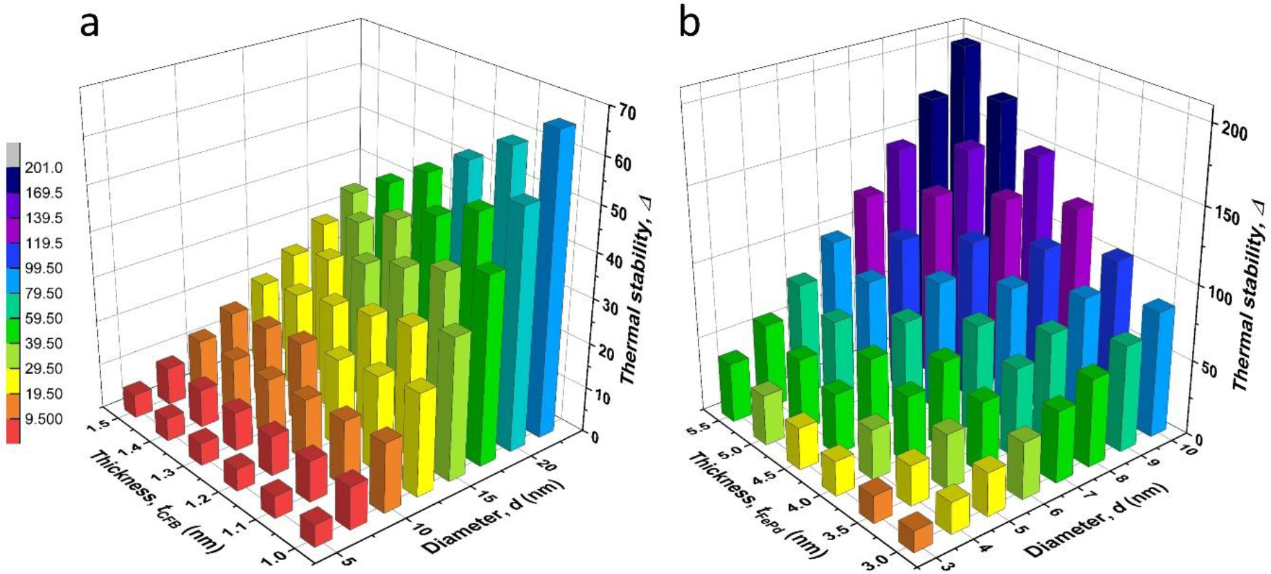
Thermal stability scales as a function of film thickness and device diameter. a) In the t regime where interfacial PMA makes CoFeB perpendicularly magnetized (tCFB ~1.3 nm), Δ is always less than 20 at d ≤ 10 nm. b) Thanks to its strong bulk PMA, L10-FePd can sustain Δ of exceeding 60 at a moderate tFePd ~5 nm while downscaling to d = 5 nm. The parameters of CoFeB and L10-FePd are assumed to be Ki,CFB = 1.5 mJ m−2, Kb,FePd = 1.7 MJ m−3, and saturation magnetization MS,CFB = 1.2 MA m−1 and MS,FePd = 1.1 MA m−1, respectively.
L10-FePd manifests strong bulk PMA of Kb,FePd ~1.7 MJ m−3[23] and thus, excellent scalability. As shown in Figure 1b, Δ = 60 that corresponds to ~10 yr data retention[24] can be reached at d = 5 nm with a moderate tFePd ~5 nm. As a free layer material, L10-FePd has been applied in full p-MTJs[25,26] and read sensor-type MTJs[27] (with in-plane reference layer), in which a projected TMR up to 85% was reported. We realized an unforeseen energy efficiency in bipolar electric-field switched FePd p-MTJs through voltage-controlled exchange coupling and achieved an ultralow J ~1.1 × 10⁵ A cm−2.[28] A recent report unveiled the chemisorption-type van der Waals force and robust interfacial PMA of FePd-Graphene interface,[29] indicating potential benefits from integrating FePd-based spintronic devices with 2D materials. Additionally, the low α of FePd[30–33] outperforms those of RE-TM compounds,[34,35] Co (or CoFe)-based multilayers,[36,37] and many other L10-alloys (e.g., L10-FePt)[32,33,38] and is highly desirable for device applications because J is proportional to α. Despite the advantages of L10-FePd, its PMA and damping depend on the crystallinity of L10 phase and (001) texture. In order to seed a strong (001)-textured L10 order, only a few special substrates, such as MgO(001)[25–28,30,31] and SrTiO3(001),[29,30] are suitable for L10-FePd growth. These substrates are costly, hard to obtain in large sizes, and most severely, incompatible to the monolithic integration with semiconductor microelectronics. As a result, applying L10-FePd to extend the scalability of spintronic devices remains impractical.
In this report, we demonstrate the success of synthesizing L10-FePd with (001) texture on industry-ready thermally-oxidized Si wafers by magnetron sputtering. Characterized by vibrating-sample magnetometry (VSM) and ultrafast time-resolved magneto-optical Kerr effect (TR-MOKE) metrology, our samples exhibit strong PMA with full out-of-plane remanence (Mr), high anisotropy field (Hk), as well as low α. X-ray diffraction (XRD) measurements confirm its L10 phase and strong (001) texture. Most importantly, the L10-FePd(001) texture is induced by a (001)-textured MgO seed layer, which was prepared by industry-compatible radio-frequency (RF) magnetron sputtering at room temperature on the amorphous SiO2 surface. Atomic-resolution scanning transmission electron microscopy (STEM) clearly reveals the epitaxial growth of buffer layer(001)/L10-FePd(001) on MgO(001). Given that MgO is a core part of the mainstream p-MTJ material system with worldwide adoptability, this research provides an accessible pathway to enable deeply-scalable spintronic applications. Moreover, we also successfully developed perpendicular-synthetic antiferromagnets (p-SAFs) that consist of two L10-FePd layers antiferromagnetically coupled through an Ir spacer. Surprisingly, the Ir-spaced FePd p-SAFs prepared on Si/SiO2 wafers exhibit very large interlayer exchange coupling (IEC, −Jex), up to ~34% higher than the previous report for the Ru-spaced p-SAF on MgO(001) substrates.[26] As p-SAFs have been predicted[39,40] and experimentally demonstrated[41–44] to perform better than uniform ferromagnets with faster speed, higher Δ, as well as lower J, this result further exhibits the technological potential of application of our study.
2. Results and Discussion
As depicted in Figure 2a, the stacks containing a Cr/Pt bilayer buffer and the FePd layer were direct-current magnetron sputtered onto Si(001)/SiO2 (300 nm, thermally oxidized) wafers with/without an RF sputtered MgO seed layer, followed by a capping layer. Except for the 5 nm MgO that was deposited in an auxiliary chamber (Oerlikon Leybold Vacuum UNIVEX MULTICHAMBER,[45] base vacuum better than 3 × 10⁻⁹ Torr) at room temperature, all the layers were prepared in a custom ultrahigh vacuum chamber with base pressure better than 5 × 10⁻¹⁰ Torr. Before the deposition of Cr, the MgO-coated wafers were baked at 600 °C for 1 h in vacuum and held for an additional 0.5 h in an 0.8 mTorr N2 environment to heal any oxygen vacancies known to form on the surface of MgO during vacuum annealing.[46] The Cr (30 nm)/Pt (4 nm) buffer and 8 nm FePd layer were grown at 350 °C with a 10 min in-situ anneal at 600 °C performed after the Cr layer deposition for stress relief. Finally, a Ru (2 nm)/Ta (3 nm) capping layer was grown after cooling the substrate down to room temperature. The sputtering was at Ar pressure of 2 mTorr, 3 mTorr, and 6 mTorr for MgO, Cr/Pt, and FePd, respectively.
Figure 2.
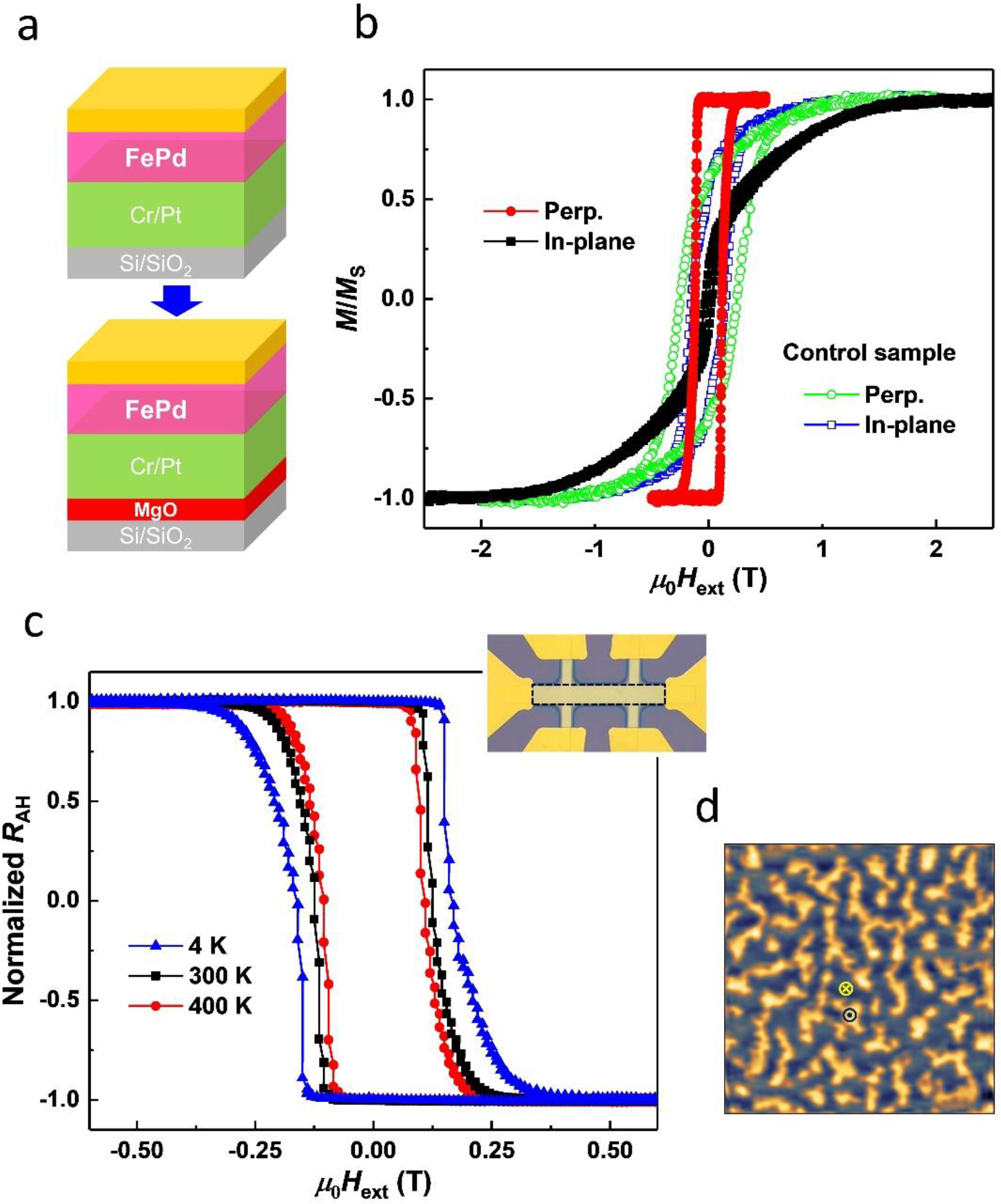
a) Stack structure of the samples with (bottom) and without (top) the MgO seed layer. The one without MgO serves as a control sample. b) Hysteresis loops of (001)-textured L10-FePd (solid symbols) and the control sample (empty symbols). c) RAH-Hext loops collected from a 10 × 78 μm2 Hall bar device at different temperatures. Inset: An optical microscopy image of the device. The Hall bar channel is labelled by black dashed line. d) A 5 × 5 μm2 MFM image of the (001)-textured L10-FePd, where the markers indicate the direction of local magnetization.
The magnetization (M)-external field (Hext) hysteresis loops of FePd layers were measured by VSM and plotted in Figure 2b. Despite the amorphous SiO2 surface, FePd shows strong PMA with Mr = MS and μ0Hk ~2 T with the insertion of MgO, indicating its (001)-textured L10 phase. By integrating over the in-plane curve, we estimate the uniaxial anisotropy energy density (Ku) to be 1.13 MJ m−3, about 60 % higher than the case of (Mn-Cr)AlGe[47,48] and comparable with results of FePd formed on MgO(001) or SrTiO3(001) substrates.[30] Compared with former efforts such as crystalizing FePdB by SSE,[49] performing long-time annealing in H2,[50] precisely controlling the heating rate,[51] trying various buffers,[52,53] and alloying FePd with Cu,[54] this study is deliberately uncomplicated and uniquely achieves distinct PMA of FePd with amorphous substrates. The control sample (i.e., without the MgO seed layer) shows a significant in-plane component of the easy axis. As the PMA follows the orientation of the (001)-textured L10 phase, the VSM measurements imply that the MgO seed layer is key to engineer the correct FePd microstructure. To futher explore its application potential, the PMA FePd was patterned into Hall bar devices by using photolithography and Ar+ ion milling. Top-contact pads made of Ti (10 nm)/Au (100 nm) were fabricated by E-beam evaporation and a lift-off process. The Hext-dependence of anomalous Hall resistance (RAH) and device geometry are presented in Figure 2c and its inset, respectively. The RAH-Hext loops collected from a cryogenic temperature of 4 K to a high temperature of 400 K show that FePd maintains its PMA in a wide temperature range. FePd-based spintronic devices, as a result, manifest a broad application prospect from superconducting circuits (~4 K)[55,56] to automotive grade-1 products (−4000B0C to 12500B0C).[57,58] Figure 2d presents a magnetic force microscopy (MFM) image of the MgO-seeded FePd film in the demagnetized state, showing the labyrinth domain structure typical of perpendicularly magnetized films.[59] The observed sub-micron magnetic domain size is comparable to those observed in FePd films grown on MgO(001) substrates.[60]
To further investigate its magnetic characteristics, particularly dynamic properties, we conducted TR-MOKE measurements on the L10-FePd(001) thin film as schematically shown in Figure 3a, where θH and θM respectively denote the direction of Hext and resulted equilibrium angle of M. Details of the TR-MOKE experimental setup and analysis can be found in our previous studies.[61,62] A representative set of TR-MOKE signals and associated fitting results are plotted in Figure 3b as functions of the time delay between pump excitation and probe sensing. The experiments are conducted under μ0Hext ranging from 1.0 to 3.1 T along θH = 84° deviating from the surface normal. Here, θH = 84° was chosen to balance the needs for precessional signal amplitudes and the measurement sensitivity to α.[61–63] Figure 3c summarizes the corresponding precession frequency (f, top panel) and relaxation time (τ, bottom panel) that are extracted from the damped magnetization oscillation observed in experiments.[64–66] The best fits of field-dependent f and τ−1 yield μ0Hk = 1.33 ± 0.06 T and α = 0.012 ± 0.007. The translucent data points are excluded from fitting to avoid the influence of the laser-induced acoustic waves (~56 GHz ± 3 GHz measured with the time-domain thermoreflectance technique) via spin-strain coupling.[67] At low fields (μ0Hext < 1.4 T), the measured τ deviate markedly from the model fit, which can be explained by the low-field loss.[68] It is noteworthy that the μ0Hk (1.33 T) derived from TR-MOKE, though still sizeable, is lower than the value (~2 T) obtained from VSM, likely due to the thermal effect of laser heating.
Figure 3.
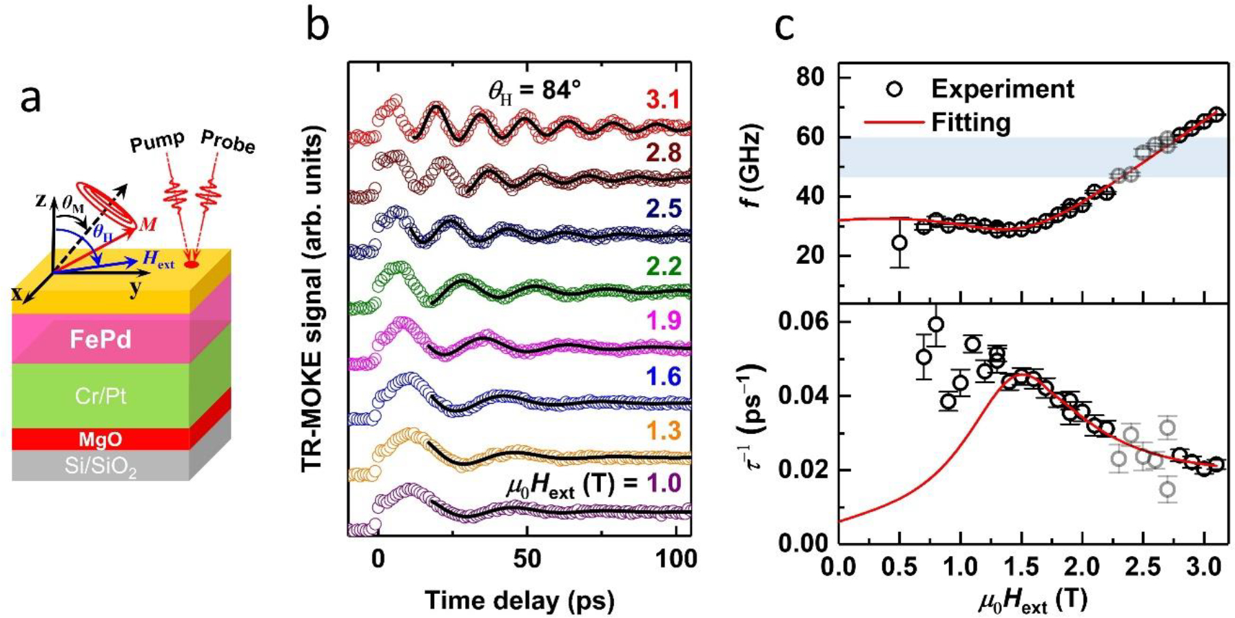
a) Schematic illustration of the TR-MOKE measurements performed on the L10-FePd(001) sample. b) TR-MOKE signals, which reflect the damped precession of M induced by laser excitation, as functions of time delay. The experimental data and fitting curves are marked by circles and lines, respectively. c) Extracted f (top panel) and τ−1 (bottom panel) vs. μ0Hext. Due to the spin-strain coupling, translucent data points (highlighted by the light blue region) are excluded from the fitting.
The crystal structures and registry between layers were explored by X-ray diffraction (XRD) studies. By using a Bruker D8 Discover microdiffractometer equipped with a Vantec 500 2D detector and a Hubber ¼ Eulerian cradle, we collected reciprocal space maps of the sample. The scattering peaks of individual layers are assigned in different panels of Figure 4a. From left to right, we identify the FePd(001) peak, confirming the strong (001) texture and L10 ordering of FePd sputtered on Si/SiO2 wafers, the Pt(002) and FePd(002) peaks, which are close to each other but still distinguishable, and the Cr(002) peak. Apparently, both the bilayer buffer and FePd obeyed (001)-textured growth on the MgO layer, which is a precondition of the high PMA and low α of L10-FePd(001). We also observed that the structural coherence of the layers is better in the direction of the growth than in the in-plane directions, which highlights the good crystalline quality of the layers despite the granular-oriented morphology imposed by the MgO layer. The high crystallinity and strong texture of the sample can be better visualized in Figure 4b, where the peak intensity in HL and KL projections (H, K and L reflect the coordinate basis associated with the crystal) are extracted, temperature-colored with a scale approximately matching the one of Figure 4a, and presented in a 3D form. The conventional θ−2θ spectrum is plotted in Figure 4c. Based on the peak positions and intensity, the out-of-plane lattice parameters of Cr, Pt, and FePd are estimated to be (2.88 ± 0.01) Å, (3.90 ± 0.03) Å, and (3.73 ± 0.02) Å, respectively, in which uncertainties are associated with pseudo-Voigt fits to the data. The L10 ordering parameter (S) of FePd is calculated to be 0.73 ± 0.01, also comparable to the counterparts using MgO(001) or SrTiO3(001) substrates.[30] The MgO peaks are not observed due to its small thickness tMgO = 5 nm and low electron density, however the crystallinity of the MgO layer is later confirmed with STEM measurements. The unlabelled peaks with very high intensity and narrow spread are from the substrate lattice.
Figure 4.

XRD patterns of the sample. a) Large area reciprocal space maps (HL projection). The scattered intensity is represented with a temperature-colored scale. b) The 3D representation of the 00L specular rod. In this representation, the scattering ellipsoids are obtained from the fitting of individual peaks in both the HL and KL projections. c) The conventional θ−2θ spectrum.
The microstructure of the MgO layer and the epitaxial relationship of the stack are studied by STEM. Figure 5a shows a cross-sectional image of the stack under the high-angle annular dark field (HAADF) mode. It is clear that both the bilayer buffer and L10-FePd followed a grain-on-grain heteroepitaxial growth on textured MgO. The grain boundaries, one of which is marked by the dashed line, are shared by the MgO seed layer, bilayer buffer, as well as FePd. This epitaxial growth is established from MgO since it tends to form (001) texture on amorphous surfaces,[69] of which CoFeB is a known example.[15] A zoomed-in image around the FePd layer and the energy dispersive X-ray (EDX) profile is shown in Figure 5b. The interfaces are flat and sharp, showing no significant interdiffusion during the sputtering and annealing processes. By taking atomic-resolution images (Figure 5c) and nanobeam diffraction (NBD) patterns (shown later), we estimate the lattice parameters of each layer and present them in Figure 5d.[70] They are consistent with the values obtained from XRD measurements. The epitaxial relationship is inferred to be MgO [100](001)/Cr [110](001)/Pt [100](001)/L10-FePd [100](001), in which the Cr/Pt buffer can effectively release the lattice misfit between MgO and L10-FePd.
Figure 5.
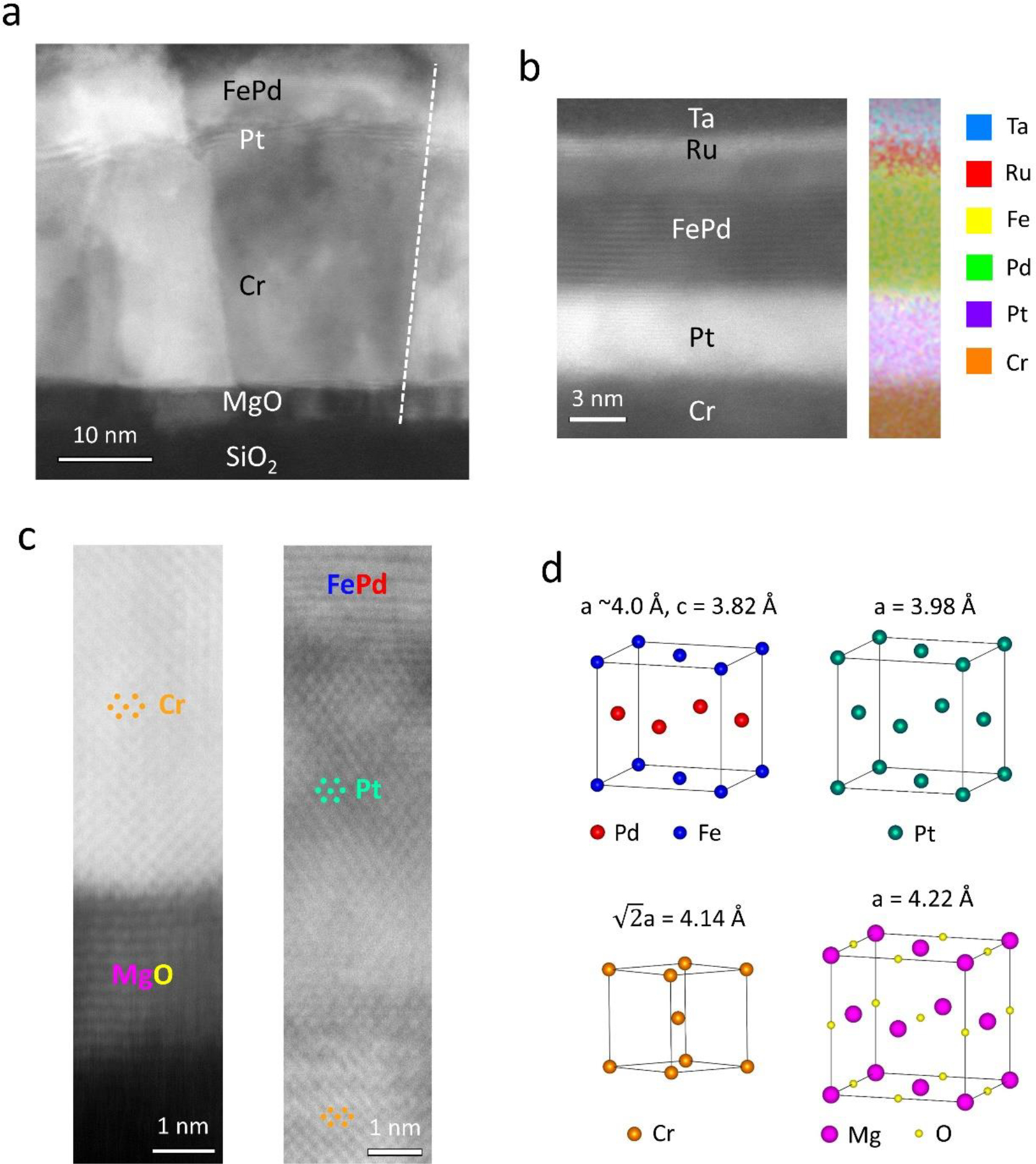
STEM images of the sample and analysis. a) A cross-sectional HAADF image of the entire stack. The dashed line marks a grain boundary. b) A zoomed-in image around the L10-FePd and EDX elemental distribution. c) Interfaces between each layer imaged at atomic resolution. d) Crystalline structures and estimated lattice parameters of L10-FePd, Pt, Ct, and MgO.
In addition, we also prepared FePd-based p-SAFs on Si/SiO2 wafers by inserting a sub-nm Ir spacer (tIr is wedged from 4.5 to 6.0 Å) between two L10-FePd layers. The samples were cleaved along the wedge direction and indexed from 1 to 12. Their M-Hext hysteresis loops, as shown in Figure 6a and 6b, indicate strong PMA with all tIr and markedly larger in-plane saturation field (by nearly 1 T magnitude) compared to the out-of-plane saturation field. That is, both the top and bottom FePd layers are (001)-textured. By increasing tIr, the M-Hext loop gradually changes from a compensated antiferromagnetic configuration[71] (Sample 1) to a ferromagnetic-like configuration in which two FePd layers reverse almost coherently (Sample 12). That means, within the tIr range of this study, a monotonic decrease of IEC strength as tIr increases. Based on SAF magnetization switching behaviors, the top FePd layer is found to switch first as it was prepared to be thinner (3 nm) than the bottom FePd layer (6 nm). In the M-Hext loops of low index samples, the gradual transition of the magnetizations from antiparallel to parallel is consistent with the magnetic free energy of a p-SAF with Ku near parity with –Jex/tFePd,top.[71] Since overcoming PMA to rotate L10-FePd layers into the plane and IEC to force them aligned cost certain amounts of Zeeman energy, the anisotropy and exchange fields should be approximately additive.[72] Assuming the intrinsic magnetic properties of L10-FePd layers remain constant among such a narrow tIr range of only ~1.5 Å, the areas contoured by two in-plane hysteresis curves should reflect their difference in the IEC energy. Therefore, it is also observed that −Jex decreases as tIr increases. To quantitatively measure −Jex, the TR-MOKE technique was employed to study the p-SAFs[73] as a function of tIr. Capable of measuring dynamics up to the THz range, TR-MOKE is a powerful tool to characterize p-SAFs with high PMA and IEC. By fitting the field-dependent f in the high- (HF) and low-frequency (LF) modes, Jex can be calculated by Jex = J1 + 2J2, with J1 and J2 the extracted bilinear and biquadratic exchange coupling constants, respectively.[73,74] As a representative example, Figure 6c shows the field-dependence of f in both precessional modes of Sample 1. The fitting curve gives −Jex = 3.48 ± 1.09 mJ m−2, which is ~34% larger compared to the former result.[26] In Figure 6d, −Jex is plotted as a function of sample index and nominal tIr. In agreement with VSM results, −Jex decreases as tIr increases, indicating the coverage of tIr by the first (and strongest) antiferromagnetic range of Ir’s Ruderman-Kittel-Kasuya-Yosida (RKKY) oscillation.[75] A sketch of the p-SAF trilayer and TR-MOKE metrology is shown as the inset of Figure 6d. Given the multiple advantages of p-SAFs over single-magnet counterparts,[39–44] the FePd-based p-SAFs prepared on Si/SiO2 wafers can further advance the application of scalable spintronic devices.
Figure 6.
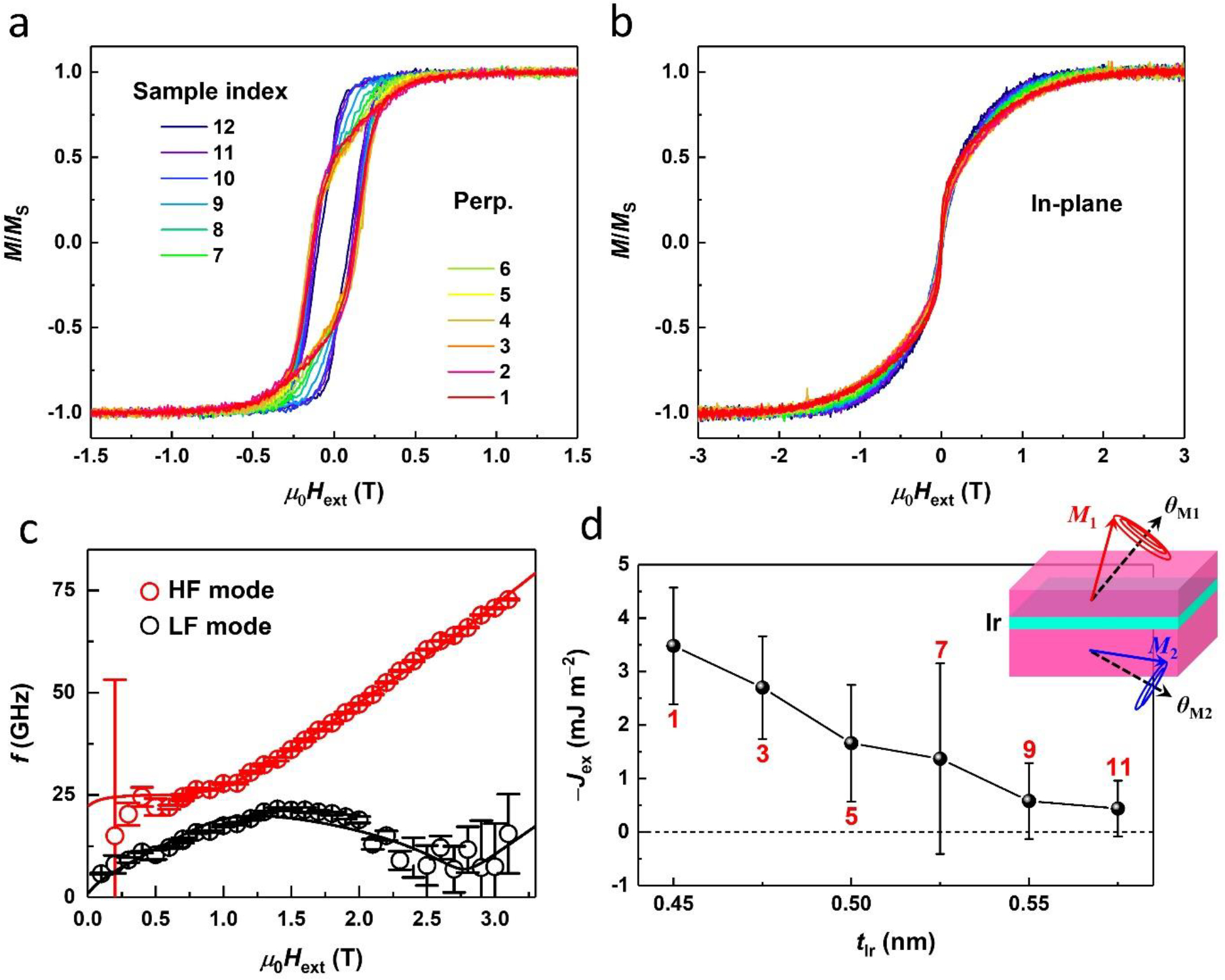
Hysteresis loops of FePd-based p-SAFs under a) perpendicular and b) in-plane Hext. c) Field-dependent f of HF and LF in Sample 1 (θH = 85°). Circles and lines denote measurement data and theoretical fits, respectively. d) −Jex of FePd-based p-SAFs vs. sample index (numbers in red) and nominal tIr. Inset: Schematic of high-fidelity TR-MOKE metrology developed to study p-SAFs. M1, M2, θM1, and θM2 denote the magnetization of the top and bottom L10-FePd layers and their equilibrium angles under Hext, respectively.
The significant enhancement of −Jex is attributed to the strong RKKY interaction of Ir as well as proper seed and buffer layers of L10-FePd on amorphous SiO2 surface. To elucidate the high performance of L10-FePd/Ir/L10-FePd p-SAFs, we performed high-resolution transmission electron microscopy (HRTEM) and STEM to investigate their microstructure. As shown in Figure 7a, the high crystallinity of both the top and bottom FePd layers is confirmed. Though the Ir spacer is ultrathin, it is still observable. By using the STEM-HAADF mode, the Ir spacer can be imaged with better contrast as shown in Figure 7b, where the two FePd slabs are separated by a continuous Ir band. To convincingly illustrate the epitaxial relationship between each layer, especially the two FePd layers, we conducted NBD measurements to a single grain. The results, as presented in Figure 7c, show a grain-on-grain heteroepitaxy through the Ir layer. Specifically, the SAF trilayer is textured as L10-FePd [100](001)/Ir/L10-FePd [100](001). Such an epitaxial growth, together with the sharp and flat interfaces between each layer, enables the considerable improvement in −Jex.
Figure 7.
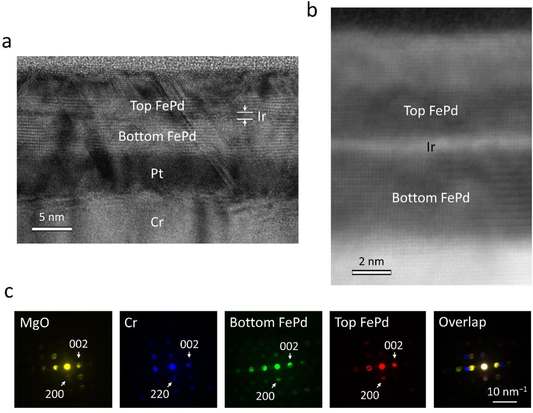
a) A cross-sectional HRTEM image of the FePd-based p-SAF. b) A STEM-HAADF image of the L10-FePd/Ir/L10-FePd trilayer structure. c) NBD patterns collected within a single grain and their overlap.
3. Conclusions
In summary, high-quality L10-FePd(001) thin films were deposited on industry-compatible Si/SiO2 wafers. Without expensive MgO(001) or SrTiO3(001) substrates, the FePd thin films still possess strong PMA and low α with suitable seed and buffer layers. Furthermore, by adding an Ir spacer, p-SAFs with markedly improved IEC were also achieved. The high performance of both the L10-FePd single layer and its SAF indicates high crystallinity, strong (001) texture, as well as an epitaxial growth on amorphous SiO2 surface. Comprehensive characterizations were performed to reveal the lattice details of the MgO seed layer, Cr/Pt bilayer buffer, L10-FePd, and its SAF and the epitaxial relationship throughout the stack. As MgO, the crucial seed layer material in this study, has been widely used by the spintronics community and is deposited by conventional RF sputtering, our results removed a key obstacle of applying L10-FePd for deeply-scalable spintronic devices.
Acknowledgements
This work was supported in part by the Defense Advanced Research Projects Agency (DARPA) (Advanced MTJs for computation in and near random access memory) under Grant HR001117S0056-FP-042, in part by the National Institute of Standards and Technology (NIST), in part by SMART, one of seven centers of nCORE, a Semiconductor Research Corporation program, sponsored by NIST, in part by the Minnesota Nano Center by the National Science Foundation (NSF) through the National Nanotechnology Coordinated Infrastructure (NNCI) under Award ECCS-2025124, and in part by the Characterization Facility of University of Minnesota by NSF through the UMN MRSEC under Grant No. DMR-2011401. D.L. and J.-P.W. thank the support from the Office of the Vice President for Research (OVPR) of the University of Minnesota to the purchase of the ultrahigh-vacuum multi-chamber sputtering system (Oerlikon Leybold Vacuum UNIVEX MULTICHAMBER). D.H. and X.W. appreciate the partial support from NSF under Grant No. CBET- 2226579. The authors thank the team of Covalent Metrology for performing TEM-related characterizations.
Contributor Information
Deyuan Lyu, Department of Electrical and Computer Engineering, University of Minnesota, Minneapolis, MN 55455, USA.
Jenae E. Shoup, Materials Science and Engineering Division, National Institute of Standards and Technology, Gaithersburg, MD 20899, USA
Dingbin Huang, Department of Mechanical Engineering, University of Minnesota, Minneapolis, MN 55455, USA.
Javier García-Barriocanal, Characterization Facility, University of Minnesota, Minneapolis, MN 55455, USA.
Qi Jia, Department of Electrical and Computer Engineering, University of Minnesota, Minneapolis, MN 55455, USA.
William Echtenkamp, Department of Electrical and Computer Engineering, University of Minnesota, Minneapolis, MN 55455, USA.
Geoffrey A. Rojas, Characterization Facility, University of Minnesota, Minneapolis, MN 55455, USA
Guichuan Yu, Characterization Facility, University of Minnesota, Minneapolis, MN 55455, USA.
Brandon R. Zink, Department of Electrical and Computer Engineering, University of Minnesota, Minneapolis, MN 55455, USA
Xiaojia Wang, Department of Mechanical Engineering, University of Minnesota, Minneapolis, MN 55455, USA
Daniel B. Gopman, Materials Science and Engineering Division, National Institute of Standards and Technology, Gaithersburg, MD 20899, USA
Jian-Ping Wang, Department of Electrical and Computer Engineering, University of Minnesota, Minneapolis, MN 55455, USA
References
- [1].Mangin S, Ravelosona D, Katine JA, Carey MJ, Terris BD, and Fullerton EE, Nat. Mater. 2006, 5, 210. [DOI] [PubMed] [Google Scholar]
- [2].Meng H and Wang J-P, Appl. Phys. Lett. 2006, 88, 172506. [Google Scholar]
- [3].Kent AD, Özyilmaz B, and del Barco E, Appl. Phys. Lett. 2004, 84, 3897. [Google Scholar]
- [4].Lee KJ and Redon O, Appl. Phys. Lett. 2005, 86, 022505. [Google Scholar]
- [5].Nishimura N, Hirai T, Koganei A, Ikeda T, Okano K, Sekiguchi Y, and Osada Y, J. Appl. Phys. 2002, 91, 5246. [Google Scholar]
- [6].Nakayama M, Kai T, Shimomura N, Amano M, Kitagawa E, Nagase T, Yoshikawa M, Kishi T, Ikegawa S, and Yoda H, J. Appl. Phys. 2008, 103, 07A710. [Google Scholar]
- [7].Ye L-X, Lee C-M, Lai J-H, Canizo-Cabrera A, Chen W-J, and Wu T.-h., J. Magn. Magn. Mater. 2010, 322, L9. [Google Scholar]
- [8].Nistor LE, Rodmacq B, Auffret S, and Dieny B, Appl. Phys. Lett. 2009, 94, 012512. [Google Scholar]
- [9].Tadisina ZR, Natarajarathinam A, and Gupta S, J. Vac. Sci. Technol. A 2010, 28, 973. [Google Scholar]
- [10].Yakushiji K, Saruya T, Kubota H, Fukushima A, Nagahama T, Yuasa S, and Ando K, Appl. Phys. Lett. 2010, 97, 232508. [Google Scholar]
- [11].Carvello B, Ducruet C, Rodmacq B, Auffret S, Gautier E, Gaudin G, and Dieny B, Appl. Phys. Lett. 2008, 92, 102508. [Google Scholar]
- [12].Kim G, Sakuraba Y, Oogane M, Ando Y, and Miyazaki T, Appl. Phys. Lett. 2008, 92, 172502. [Google Scholar]
- [13].Kishi T, Yoda H, Kai T, Nagase T, Kitagawa E, Yoshikawa M, Nishiyama K, Daibou T, Nagamine M, Amano M, Takahashi S, Nakayama M, Shimomura N, Aikawa H, Ikegawa S, Yuasa S, Yakushiji K, Kubota H, Fukushima A, Oogane M, Miyazaki T, and Ando K, in Proc. IEEE Int. Electron. Devices Meeting (IEDM), San Francisco, CA, USA, Dec. 2008. [Google Scholar]
- [14].de Person P, Warin P, Jamet M, Beigne C, and Samson Y, Phys. Rev. B 2007, 76, 184402. [Google Scholar]
- [15].Wang Z, Saito M, McKenna KP, Fukami S, Sato H, Ikeda S, Ohno H, and Ikuhara Y, Nano Lett. 2016, 16, 1530. [DOI] [PubMed] [Google Scholar]
- [16].Yuasa S, Nagahama T, Fukushima A, Suzuki Y, and Ando K, Nat. Mater. 2004, 3, 868. [DOI] [PubMed] [Google Scholar]
- [17].Parkin SSP, Kaiser C, Panchula A, Rice PM, Hughes B, Samant M, and Yang S-H, Nat. Mater. 2004, 3, 862. [DOI] [PubMed] [Google Scholar]
- [18].Ikeda S, Miura K, Yamamoto H, Mizunuma K, Gan HD, Endo M, Kanai S, Hayakawa J, Matsukura F, and Ohno H, Nat. Mater. 2010, 9, 721. [DOI] [PubMed] [Google Scholar]
- [19].Chun KC, Zhao H, Harms JD, Kim T-H, Wang J-P, and Kim CH, IEEE J. Solid-State Circuits 2013, 48, 598. [Google Scholar]
- [20].Peng S, Kang W, Wang M, Cao K, Zhao X, Wang L, Zhang Y, Zhang Y, Zhou Y, Wang KL, and Zhao W, IEEE Magn. Lett. 2017, 8, 3105805. [Google Scholar]
- [21].Watanabe K, Jinnai B, Fukami S, Sato H, and Ohno H, Nat. Commun. 2018, 9, 663. [DOI] [PMC free article] [PubMed] [Google Scholar]
- [22].Jinnai B, Igarashi J, Watanabe K, Funatsu T, Sato H, Fukami S, and Ohno H, in Proc. IEEE Int. Electron. Devices Meeting (IEDM), San Francisco, CA, USA, Dec. 2020. [Google Scholar]
- [23].Klemmer T, Hoydick D, Okumura H, Zhang B, and Soffa WA, Scr. Metall. Mater. 1995, 33, 1793. [Google Scholar]
- [24].Chen E, Apalkov D, Diao Z, Driskill-Smith A, Druist D, Lottis D, Nikitin V, Tang X, Watts S, Wang S, Wolf SA, Ghosh AW, Lu JW, Poon SJ, Stan M, Butler WH, Gupta S, Mewes CKA, Mewes T, and Visscher PB, IEEE Trans. Magn. 2010, 46, 1873. [Google Scholar]
- [25].Zhang D-L, Schliep KB, Wu RJ, Quarterman P, Hickey DR, Lv Y, Chao X, Li H, Chen J-Y, Zhao Z, Jamali M, Mkhoyan KA, and Wang J-P, Appl. Phys. Lett. 2018, 112, 152401. [Google Scholar]
- [26].Zhang D-L, Sun C, Lv Y, Schliep KB, Zhao Z, Chen J-Y, Voyles PM, and Wang J-P, Phys. Rev. Appl. 2018, 9, 044028. [Google Scholar]
- [27].Naganuma H, Kim G, Kawada Y, Inami N, Hatakeyama K, Iihama S, Islam KMN, Oogane M, Mizukami S, and Ando Y, Nano Lett. 2015, 15, 623. [DOI] [PubMed] [Google Scholar]
- [28].Zhang D, Bapna M, Jiang W, Sousa D, Liao Y-C, Zhao Z, Lv Y, Sahu P, Lyu D, Naeemi A, Low T, Majetich SA, and Wang J-P, Nano Lett. 2022, 22, 622. [DOI] [PubMed] [Google Scholar]
- [29].Naganuma H, Nishijima M, Adachi H, Uemoto M, Shinya H, Yasui S, Morioka H, Hirata A, Godel F, Martin M-B, Dlubak B, Seneor P, and Amemiya K, ACS Nano 2022, 16, 4139. [DOI] [PMC free article] [PubMed] [Google Scholar]
- [30].Iihama S, Sakuma A, Naganuma H, Oogane M, Mizukami S, and Ando Y, Phys. Rev. B 2016, 94, 174425. [Google Scholar]
- [31].Wang X, Krylyuk S, Josell D, Zhang D, Lyu D, Wang J-P, and Gopman DB, AIP Adv. 2021, 11, 025106. [Google Scholar]
- [32].He P, Ma X, Zhang JW, Zhao HB, Lüpke G, Shi Z, and Zhou SM, Phys. Rev. Lett. 2013, 110, 077203. [DOI] [PubMed] [Google Scholar]
- [33].Qu T and Victora RH, Appl. Phys. Lett. 2015, 106, 072404. [Google Scholar]
- [34].Kim D-H, Okuno T, Kim SK, Oh S-H, Nishimura T, Hirata Y, Futakawa Y, Yoshikawa H, Tsukamoto A, Tserkovnyak Y, Shiota Y, Moriyama T, Kim K-J, Lee K-J, and Ono T, Phys. Rev. Lett. 2019, 122, 127203. [DOI] [PubMed] [Google Scholar]
- [35].Bainsla L, Kumar A, Awad AA, Wang C, Zahedinejad M, Behera N, Fulara H, Khymyn R, Houshang A, Weissenrieder J, and Åkerman J, Adv. Funct. Mater. 2022, 32, 2111693. [Google Scholar]
- [36].Kato T, Matsumoto Y, Kashima S, Okamoto S, Kikuchi N, Iwata S, Kitakami O, and Tsunashima S, IEEE Trans. Magn. 2012, 48, 3288. [Google Scholar]
- [37].Shaw JM, Nembach HT, and Silva TJ, Phys. Rev. B 2012, 85, 054412. [Google Scholar]
- [38].Mizukami S, Iihama S, Inami N, Hiratsuka T, Kim G, Naganuma H, Oogane M, and Ando Y, Appl. Phys. Lett. 2011, 98, 052501. [Google Scholar]
- [39].Camsari KY, Pervaiz AZ, Faria R, Marinero EE, and Datta S, IEEE Magn. Lett. 2016, 7, 3107205. [Google Scholar]
- [40].Yamada K, Kubota K, and Nakatani Y, J. Appl. Phys. 2020, 127, 133906. [Google Scholar]
- [41].Raymenants E, Bultynck O, Wan D, Devolder T, Garello K, Souriau L, Thiam A, Tsvetanova D, Canvel Y, Nikonov DE, Young IA, Heyns M, Soree B, Asselberghs I, Radu I, Couet S, and Nguyen VD, Nat. Electron. 2021, 4, 392. [Google Scholar]
- [42].Yoshida C, Takenaga T, Iba Y, Yamazaki Y, Noshiro H, Tsunoda K, Hatada A, Nakabayashi M, Takahashi A, Aoki M, and Sugii T, IEEE Trans. Magn. 2013, 49, 4363. [Google Scholar]
- [43].Yang S-H, Ryu K-S, and Parkin S, Nat. Nanotech. 2015, 10, 221. [DOI] [PubMed] [Google Scholar]
- [44].Lyu D, Zhang D, Gopman DB, Lv Y, Benally OJ, and Wang J-P, Appl. Phys. Lett. 2022, 120, 012404. [Google Scholar]
- [45]. Certain commercial equipment, instruments, or materials are identified in this paper in order to specify the experimental procedure adequately. Such identification is not intended to imply recommendation or endorsement by NIST, nor is it intended to imply that the materials or equipment identified are necessarily the best available for the purpose.
- [46].Suzuki I, Kubo S, Sepehri-Amin H, and Takahashi YK, ACS Appl. Mater. Interfaces 2021, 13, 16620. [DOI] [PubMed] [Google Scholar]
- [47].Kubota T, Ito K, Umetsu RY, and Takanashi K, Appl. Phys. Lett. 2021, 118, 262404. [Google Scholar]
- [48].Sasaki Y, Hiramatsu R, Kota Y, Kubota T, Sonobe Y, Sakuma A, Takanashi K, Kasai S, and Takahashi YK, Small 2022, 18, 2200378. [DOI] [PubMed] [Google Scholar]
- [49].Choi G-M, Min B-C, and Shin K-H, Appl. Phys. Lett. 2010, 97, 202503. [Google Scholar]
- [50].Ichitsubo T, Takashima S, Matsubara E, Tamada Y, and Ono T, Appl. Phys. Lett. 2010, 97, 182508. [Google Scholar]
- [51].Sun A-C, Hsu K-A, and Huang C-F, IEEE Trans. Magn. 2013, 50, 2300804. [Google Scholar]
- [52].Chang HW, Yuan FT, Chen WC, Wei DH, Lin MC, Su CC, Wang CR, Shih CW, Chang WC, and Yao YD, IEEE Trans. Magn. 2015, 51, 2102904. [Google Scholar]
- [53].Li B, Liu W, Zhao XG, Ma S, Gong WJ, Feng JN, Wang F, and Zhang ZD, Mater. Lett. 2013, 100, 58. [Google Scholar]
- [54].Polit A, Makarov D, Brombacher C, Krupinski M, Perzanowski M, Zabila Y, Albrecht M, and Marszałek M, J. Magn. Magn. Mater. 2015, 381, 316. [Google Scholar]
- [55].Lyu D, Khanal P, Lv Y, Zhou B, Yun H, Jia Q, Zink BR, Fan Y, Mkhoyan KA, Wang W, and Wang J-P, IEEE Electron Device Lett. 2022, 43, 1215. [Google Scholar]
- [56].Rehm L, Wolf G, Kardasz B, Pinarbasi M, and Kent AD, Appl. Phys. Lett. 2019, 115, 182404. [Google Scholar]
- [57].Lee K, Chao R, Yamane K, Naik VB, Yang H, Kwon J, Chung NL, Jang SH, Behin-Aein B, Lim JH, S. K, Liu B, Toh EH, Gan KW, Zeng D, Thiyagarajah N, Goh LC, Ling T, Ting JW, Hwang J, Zhang L, Low R, Krishnan R, Zhang L, L Tan S, You YS, Seet CS, Cong H, Wong J, Woo ST, Quek E, and Siah SY, in Proc. IEEE Int. Electron. Devices Meeting (IEDM), San Francisco, CA, USA, Dec. 2018. [Google Scholar]
- [58].Naik VB, Yamane K, Lee TY, Kwon J, Chao R, Lim JH, Chung NL, Behin-Aein B, Hau LY, Zeng D, Otani Y, Chiang C, Huang Y, Pu L, Jang SH, Neo WP, Dixit H, S. K, Goh LC, Toh EH, Ling T, Hwang J, Ting JW, Zhang L, Low R, Zhang L, Lee CG, Balasankaran N, Tan F, Gan KW, Yoon H, Congedo G, Mueller J, Pfefferling B, Kallensee O, Vogel A, Kriegerstein V, Merbeth T, Seet CS, Ong S, Xu J, Wong J, You YS, Woo ST, Chan TH, Quek E, and Siah SY, in Proc. IEEE Int. Electron. Devices Meeting (IEDM), San Francisco, CA, USA, Dec. 2020. [Google Scholar]
- [59].Hierro-Rodriguez A, Cid R, Vélez M, Rodriguez-Rodriguez G, Martín JI, Álvarez-Prado LM, and Alameda JM, Phys. Rev. Lett. 2012, 109, 117202. [DOI] [PubMed] [Google Scholar]
- [60].Dürr HA, Dudzik E, Dhesi SS, Goedkoop JB, van der Laan G, Belakhovsky M, Mocuta C, Marty A, and Samson Y, Science 1999, 284, 2166. [DOI] [PubMed] [Google Scholar]
- [61].Huang D, Lattery D, and Wang X, ACS Appl. Electron. Mater. 2021, 3, 119. [Google Scholar]
- [62].Lattery DM, Zhu J, Huang D, and Wang X, in Nanoscale Energy Transport, Emerging Phenomena, Methods, and Applications (Ed. Liao B), IOP Publishing, Bristol, United Kingdom, 2020, Ch. 9. [Google Scholar]
- [63].Lattery DM, Zhu J, Zhang D, Wang J-P, Crowell PA, and Wang X, Appl. Phys. Lett. 2018, 113, 162405. [Google Scholar]
- [64].Lattery DM, Zhang D, Zhu J, Hang X, Wang J-P, and Wang X, Sci. Rep. 2018, 8, 13395. [DOI] [PMC free article] [PubMed] [Google Scholar]
- [65].Zhang D, Huang D, Wu RJ, Lattery D, Liu J, Wang X, Gopman DB, Mkhoyan KA, Wang J-P, and Wang X, Appl. Phys. Lett. 2020, 117, 082405. [DOI] [PMC free article] [PubMed] [Google Scholar]
- [66].Huang D, Lyu D, Wang X, Katz MB, Zhang D, Wang J-P, Gopman DB, and Wang X, Phys. Rev. Mater. 2022, 6, 113402. [Google Scholar]
- [67].Zhang D-L, Zhu J, Qu T, Lattery DM, Victora RH, Wang X, and Wang J-P, Sci. Adv. 2020, 6, eabb4607. [DOI] [PMC free article] [PubMed] [Google Scholar]
- [68].Beaujour J-M, Ravelosona D, Tudosa I, Fullerton EE, and Kent AD, Phys. Rev. B 2009, 80, 180415(R). [Google Scholar]
- [69].Zepeda-Ruiz LA and Srolovitz DJ, J. Appl. Phys. 2002, 91, 10169. [Google Scholar]
- [70].Momma K and Izumi F, J. Appl. Crystallogr. 2011, 44, 1272. [Google Scholar]
- [71].Bloemen PJH, van Kesteren HW, Swagten HJM, and de Jonge WJM, Phy. Rev. B 1994, 50, 13505. [DOI] [PubMed] [Google Scholar]
- [72].Lau Y-C, Chi Z, Taniguchi T, Kawaguchi M, Shibata G, Kawamura N, Suzuki M, Fukami S, Fujimori A, Ohno H, and Hayashi M, Phys. Rev. Mater. 2019, 3, 104419. [Google Scholar]
- [73].Huang D, Zhang D, Wang J-P, and Wang X, arXiv: 2211.07744, version 1, submitted: Nov. 2022. [Google Scholar]
- [74].Kamimaki A, Iihama S, Taniguchi T, and Mizukami S, Appl. Phys. Lett. 2019, 115, 132402. [Google Scholar]
- [75].Yakushiji K, Sugihara A, Fukushima A, Kubota H, and Yuasa S, Appl. Phys. Lett. 2017, 110, 092406. [Google Scholar]