Abstract
Patterning is crucial for the large-scale application of functional materials. Laser-induced transfer is an emerging patterning method for additively depositing functional materials to the target acceptor. With the rapid development of laser technologies, this laser printing method emerges as a versatile method to deposit functional materials in either liquid or solid format. The emerging applications such as solar interfacial evaporation, solar cells, light-emitting diodes, sensors, high-output synthesis, and other fields are rising fields benefiting from laser-induced transfer. Following a brief introduction to the principles of laser-induced transfer, this review will comprehensively deliberate this novel additive manufacturing method, including preparing the donor layer and the applications, advantages, and limitations of this technique. Finally, perspectives for handling current and future functional materials using laser-induced transfer will also be discussed. Non-experts in laser technologies can also gain insights into this prevailing laser-induced transfer process, which may inspire their future research.
Keywords: Laser-induced transfer, Functional materials, Laser-induced forward transfer, Laser-induced thermal imaging, Laser-induced backward transfer
Introduction
Laser-induced transfer is a patterning method whereby photon-momentum prints target materials from one substrate (the donor) to another (the acceptor). After irradiation with the laser, the material is printed from the donor to the acceptor layer, as shown in Fig. 1. Laser-induced transfer can make flexible electronics, 3D constructions, and nanoparticle patterns. All the metals, semiconductors, and dielectric materials are appropriate for laser-induced transfer. The main advantage of this patterning method is to rapidly and accurately place materials onto a substrate due to contactless transfer and precisely controlled laser scanning.
Fig. 1.
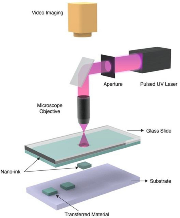
Schematic illustration of the main components in a laser-induced forward transfer or LIFT system
The key to successful transfer is the laser absorptivity of donor materials. Sufficiently high absorption is needed to convert the input laser energy into the directional movement of the functional materials for the printing process. The molecule structures and nano-morphologies of materials as well as the wavelengths of applied lasers determine the light absorptions of donor materials. The ultraviolet-visible (UV–VIS) spectrum characterization can be used to estimate the light absorptivity of the materials at a certain wavelength. Current laser sources provide a wide wavelength range from deep ultraviolet (UV) to visible and infrared (IR) bands. After an optimized wavelength is found, the selected laser can interact with the donor materials, generating sufficient transfer momentum.
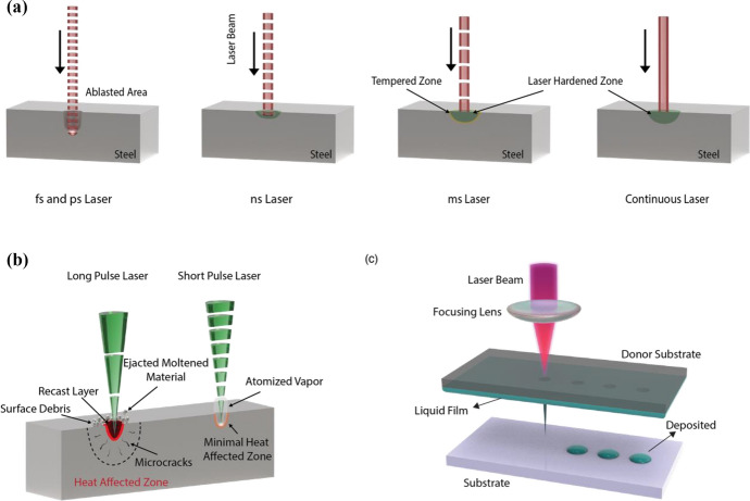
Two mechanisms are commonly used for laser transfer: momentum and thermal effect. Momentum-type laser transfer uses the momentum of the photon for the transfer. The photon is a type of boson according to the particle physics definition [1]. Compared with fermions (electrons, atoms, etc.), the photon has momentum determined only by frequency. The momentum of the light, because of the photon, can contribute to the dynamic of other tangible objects. One example is optical tweezers, where the photon momentum contributes to the object’s movement [2]. The photon momentum will contribute to the atom’s motion after being illuminated for the momentum-type laser-induced transfer. When a huge number of photons hit the donor layer, their momentums will be transferred to the donor materials, which causes the ejection of donor materials toward the acceptor. Usually, high-power and short-pulse lasers are needed to transfer momentum types, such as nanosecond, picosecond, or even femtosecond lasers. (Fig. 2).
Fig. 2.
a Schematic illustration of different types of lasers with LIFT. b Schematic illustration of long and short-pulsed lasers with LIFT. c Schematic illustration of the LIFT of liquid film with the jetting dynamics. Droplets are printed and deposited onto a receiver substrate translating from left to right
The thermal effect is another mechanism driving laser-induced transfer. Rather than using the momentum of an ultra-short laser pulse, the thermal effect transfer uses the thermodynamic energy generated from the transient local laser heating. The ultra-short laser pulse can create a transient ultra-high temperature, leading to rapid local thermal vaporization. The generated vapor and plasma will rapidly explode and drive the ejection of fragmented donor materials. Some materials will be thermally decomposed when the laser heating is sufficiently strong. The generated gas in this process will also contribute to explosion and ejection. When using a picosecond or femtosecond pulse laser, a Coulomb explosion will also occur and contribute to the transfer. According to the thermal sensitivity of the transfer materials, two subcategories of thermally laser-induced transfer have been proposed, including direct transfer and sacrificial-layer-assisted transfer. In the latter, a sacrificial layer called the dynamic release layer can absorb the photon power, generating sufficient thermodynamic energy for transferring highly temperature-sensitive materials, even living cells with narrow temperature variation tolerance [3].
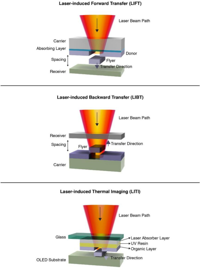
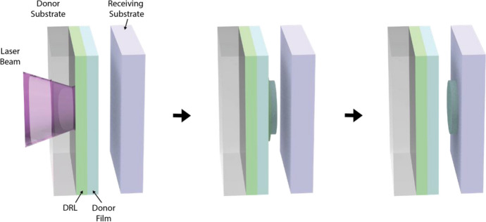
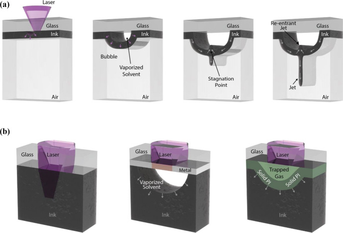
Laser-induced thermal imaging (LITI), laser-induced forward transfer (LIFT), and laser-induced backward transfer (LIBT) are the most often used laser-induced transfer techniques for printing functional materials, as shown in Fig. 3. Usually, there is a spacing between the donor and the acceptor layer. When the spacing is zero, this process can be considered as LITI. Suppose the position of the donor and acceptor is switched. In that case, that is, when the photons from the laser firstly illuminate through the acceptor layer and focus on the donor layer, and the functional materials can be delivered from the lower donor layer to the upper acceptor layer in this backward way, it is so-called LIBT. Both the contact and non-contact LIBT have been reported. Heat-labile materials can also be transferred using a sacrificial laser absorber layer; the so-called dynamic-release layer, DRL (Fig. 4). When a pulse laser illuminates on the dynamic release layer, the sacrificial materials will vaporize or decompose into gas. The generated explosion will lead to the ejection and selective transfer of donor materials. Additionally, the donor liquid layer (e.g., an ink layer) coated on an optically-clear substrate can also be selectively transferred onto the acceptor through a laser-induced ejection mechanism (Fig. 5).
Fig. 3.
Schematic illustrations of a laser-induced forward transfer (LIFT), b laser-induced backward transfer (LIBT), and c laser-induced thermal imaging (LITI)
Fig. 4.
Schematic illustration of LIFT with a dynamic release layer (DRL). The donor substrate is pre-coated with a DRL, which will vaporize or decompose into gas under laser irradiation. The generated explosion will lead to the ejection and selective transfer of donor materials
Fig. 5.
a Schematic illustration of bubble expansion and jet formation in the LIFT of liquid donor film. b Schematic illustration of different laser absorption processes during the LIFT of liquid donor films
This review will discuss the materials involved in the emerging laser-induced transfer techniques, their vast applications, advantages compared with other patterning methods for functional materials, and future perspectives.
Preparation of the Donor Layer
The donor layer should have sufficient flatness for delivering high-quality and repeatable transfers. The donor layer’s reported preparation can be divided into solution-based fabrications, physical vapor deposition, and combinational methods. Additionally, some commercial materials can be directly used as donor layers.
Solution-Based Fabrications
Solution-based fabrications have the highest compatibility with wet chemistry. On the basis of the sorts of functional materials, the donor materials can either be dissolved or dispersed in the solvent. Spin coating, doctor blade coating, and drop coating are all common methods for creating donor layers.
Spin Coating
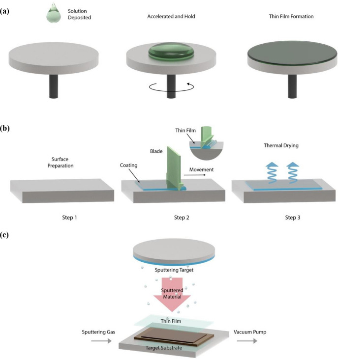
Spin coating can fabricate controllable thin films on various surfaces (Fig. 6a). Substrates are spun in the machine while a solution or dispersion is applied. Consistent, thin, and uniform films are produced by a centrifugal force caused by the spinning motion. The donor film’s thickness can be precisely controlled on various scales, from the nanometer to the micrometer, by varying the spinning speed and duration.
Fig. 6.
Schematic illustration of common methods for fabricating donor layers: a spin coating, b doctor blade coating, and c sputter deposition, one of the physical vapor deposition (PVD) methods
The spin coating was used to prepare a donor layer containing silk fibroin at 350 revolutions per minute (rpm), leading to a thickness of 3 µm [4]. Thickening agents would be used in the spin coating in some cases. Triton X-100 was mixed into the SnCl2 solution to wet the quartz substrate to enable successful spin coating [5]. Sometimes, the donor layer would be spin-coated on the substrate that can react with laser. CuCl2 aqueous solution was spin-coated on the polyimide surface, forming a donor layer for synthesizing the laser-induced graphene/CuO composite electrocatalysts by LIFT printing onto nickel foams [6]. The donor layer prepared by spin coating can also be used in LIBT. A pre-patterned waveguide relief feature was created by e-beam lithography and then transferred onto glass and polydimethylsiloxane (PDMS) substrate through LIBT [7]. The thin liquid film prepared by spin coating can also be directly used as a LIFT donor layer. To prepare single-cell isolation and cultivation, the mixture of agar and bacteria was spin-coated on a glass slide, forming a uniform donor layer for isolating the living microbial cells through LIFT [8].
Doctor Blade Coating
Doctor blade coating is another common method for fabricating thin donor films (Fig. 6 b). This method uses a doctor blade to coat the donor material slurry throughout the substrate surface with any microstructure so that the excess slurry will be wiped. After drying, a thin, uniform film is formed.
Silver ink was blade coated with a thickness of 30 µm, forming a donor layer for printing the radio frequency circuits on the glass and paper substrates through LIFT [9], and a 12 µm thick silver donor layer was also fabricated by doctor blade coating and used in LIFT to apply inverted organic photovoltaics [10]. The liquid film fabricated by doctor blade coating can also be directly used as a LIFT donor layer. Alginate in glycerin was blade coated onto a titanium-covered glass, forming a liquid donor layer with a 30 µm thickness for the LIF.[11]. This kind of LIFT can result in a depth-controlled and high-throughput liquid injection into the soft targets, called direct three-dimensional liquid delivery. Immunoglobulin G (IgG) solution containing phosphate-buffered saline (PBS) and glycerol was also blade coated onto a poly-L-lysine-covered glass, forming a 5–20 µm thick donor layer for printing biological solutions through LIFT [12, 13]. By doctor blade coating the mixture of acrylonitrile butadiene styrene (ABS) and CuO particles, the LIFT using 405 nm continuous-wave laser, can LIFT print copper interconnections onto a glass, polyimide, and paper substrate [14].
Physical Vapor Deposition
Thin films and coatings can be fabricated using physical vapor deposition (PVD). During the deposition, the target materials transfer onto the substrate as vapor, liquid, or particle, forming a uniform layer. Sputtering and evaporation are typically used.
Sputter deposition is generated by bombarding a target material with ionized gas (Fig. 6c). The following processes include the ejection of liquid or particles from the target material and deposition onto the substrate. This method can deposit metals, alloys, and compounds. Evaporation is a kind of PVD in which the deposited material is heated until evaporation. The vapor is then transported to the substrate, condensing into a thin film. Organic precursors, metals, alloys, and compounds can all be deposited as donor layers through this approach. For instance, 50 nm thick silver was deposited onto polyimide, forming a donor layer for depositing superhydrophobic nanoparticles onto N95 respirators through LIFT [15].
PVD commonly prepares a donor layer with a single element. The deposited single-element donor layers were widely used in LIFT fabrications. Magnetic sputtering depositing 60 nm thick gold film on quartz glass can be used for LIFT printing gold nanoparticles through a femtosecond laser system [16]. The 5–60 nm thick gold films were deposited through electron beam evaporation and used for LIFT printing gold onto PDMS sheets [17]. Silicon deposited on an insulator wafer with a thickness of 50 nm can LIBT print crystalline silicon nanoparticles with electromagnetic responses [18]. Additionally, the deposited donor layer can also be used to LIFT print 3D architecture (Fig. 7).
Fig. 7.
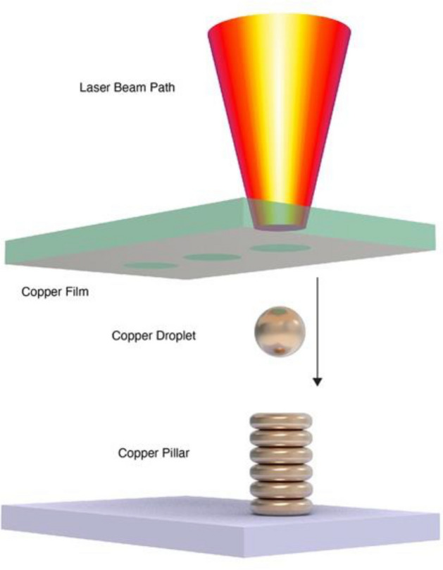
Schematic illustration of LIFT to eject liquid copper droplets and form copper pillars
Donor layers with various composites, multiple layers, or even alloy compositions can all be prepared through PVD. Alternating sputtering Zr and Pd layers onto a glass slide can form a donor layer for additive printing metallic glass microstructures [19]. Cu–Ag alloys can be deposited onto the glass slides as donor layers for printing smooth metal structures with enhanced chemical etching resistance [20, 21]. SiGe composite donor films were deposited on the borosilicate wafer through e-beam evaporation and used in the femtosecond LIFT for electrical and magnetic optical resonance applications. Nanoparticles with 200–250 nm diameters can be produced with a deposited donor film thickness of 60 nm [22]. Depositing Cu, In, and Ga layers by PVD in sequence can form a multilayer donor film that can be used in femtosecond LIFT printing for micro solar cell applications [23].
Combinational Methods
Combinational methods were also widely used to create donor films. For example, TP/Al/MEH-PPV can be fabricated by combining the PVD and spin coating, and is used in LIFT printing for organic light-emitting diode (OLED) applications [24]. An Ag nanoparticle ink donor layer had also been prepared through PVD and spin coating and used for studying the liquid jetting dynamics [25]. PVD-coated aluminum with spin-coated polytetrafluoroethylene (PTFE) was also studied for nanosecond LIFT printing the heavy metal ion sensors [26], and 80 nm thick aluminum thin films were thermally evaporated onto the triazene polymer for LIFT fabricating polymer light-emitting diode pixels [27].
Commercial Materials
Multiple commercial materials (e.g., commercial polymer films) can be directly used as the donor layer for laser-induced transfer. The aromatic compounds in polyimide can be rearranged into the graphitic structure under laser irradiating, making it a direct precursor for producing laser-induced grapheme [28]. The laser-induced graphene can be fabricated and transferred onto any substrate using a suitable pulse mode. LIFT printing of graphene on a nickel foam-based current collector can be achieved using polyimide as donor material [29]. The printed electrode delivered an areal capacitance of 1 F/cm2. Because of the superhydrophobic and oleophilic nature of the printed graphene, oil–water separation devices were also created through LIFT printing graphene onto the 3D-printed thermoplastic prototypes [30]. By depositing these graphene flakes onto the glass as a coating by LIFT, the superhydrophobic and photothermal graphene coating can kill the bacteria under solar light with an efficiency of up to 99.5% [31]. These photothermal graphene coatings can also be printed onto the cotton to enhance solar absorption for desalinating seawater into freshwater with sunlight [32]. To deposit these self-cleaning graphenes onto the thermal-sensitive surgical mask, a two-step LIFT process was developed to print graphene from polyimide onto intermediate polyimide using a high-power continuous-wave laser and then onto low-melting-point polyimide using low-power nanosecond pulse laser [33]. The mixing reactors, micro-devices for measuring droplet volume, and auto-filtering fluidic channels were printed on a high alumina silicate glass using the PTFE film as a donor [34]. Superhydrophobic structures can be created through femtosecond LIBT using a commercial fluorinated ethylene propylene film as the donor layer [35].
Advantages Compared with Other Techniques
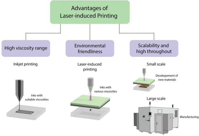
The overview of the major advantages of laser-induced transfer printing compared with other commonly used printing techniques is illustrated in Fig. 8.
Fig. 8.
Schematic illustration of advantages of laser-induced printing compared with other commonly used printing techniques
High Viscosity Range
The most commonly used method for printing functional materials is inkjet printing [36]. Current inkjet printers can only use inks with suitable viscosities for printing. Most traditional printing methods can only print those materials in the fluid state, for example, inks or melting materials. In contrast, laser-induced transfer printing allows for fluid materials with various viscosities and solid materials to be printed onto various substrates. The expanded range would make the laser-induced transfer more versatile and allow for printing in various settings.
Environmental Friendliness
The laser-induced transfer printing process can function without solvents, making it more environmentally friendly. Additionally, the most used techniques for metal printing are powder bed fusion (PBF) and direct energy deposition (DED). All these methods take a lot of energy to melt the metal and cool the equipment. By comparison, in a laser-induced transfer process, the melting and cooling processes are all finished in an ultra-short time under pulse laser irradiation. The consumed energy and generated heat are much lower, making it a more power-saving and low-carbon technique. Meanwhile, the much shorter melting and cooling processes made it more efficient.
Scalability and High-Throughput
Traditional inkjet printing and fusion-based printing techniques are usually slow and small-scale, which are limited by the nozzle movement speed, fluid extrusion rate, and material cooling rate. In contrast, in a laser-induced transfer process, the laser movement controlled by the deflection of the reflector is ultra-fast. Meanwhile, the transfer process of the material will be finished in nanoseconds. All these factors result in a high printing speed. Therefore, laser-induced transfer methods are scalable for high-throughput printing. Because of this, they are ideal for a wide range of applications, including new material development and large-scale manufacturing.
Applications
Laser-induced transfer techniques have many advanced features for printing functional materials onto desired locations. These drop-on-demand features enable the patterning of expensive materials in high precision. Laser-induced transfer printing can be applied on many acceptor substrates, including porous and non-porous surfaces. Meanwhile, metals, semiconductors, and polymers can all be used as donors for laser-induced transfer printing. The precise printing and the wide selection of donors/acceptors make laser-induced transfer an attractive technology for various applications (Figs. 9 and 10).
Fig. 9.
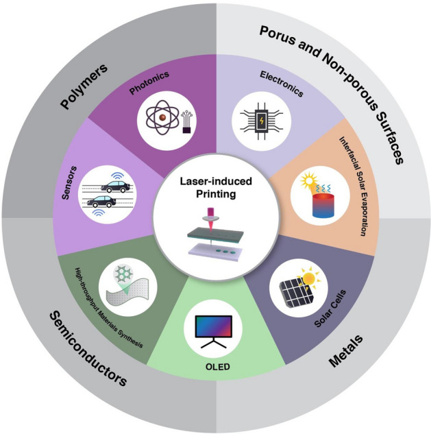
Schematic illustration of applications of laser-induced printing
Fig. 10.
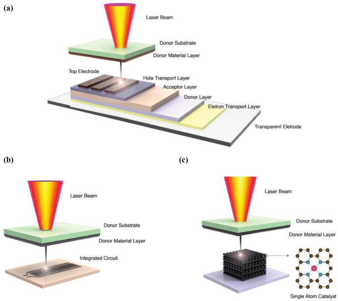
Schematic illustrations of the laser-induced transfer printing processes for a an organic photovoltaic cell, b an integrated circuit, and c a 3D graphene framework containing a library of single-atom catalysts
Interfacial Solar Evaporation
Solar distillation, also known as solar still, is a process that uses sunlight to evaporate impure water and produce fresh, potable water. Solar still can purify water from any source, including gray, brackish, and salt waters. The key technology, interfacial solar evaporation, uses the membrane with high photothermal conversion to evaporate the water with an evaporation rate of up to 10 kg/m2 h. Interfacial solar evaporation can ease the global water crisis significantly.
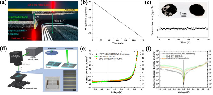
Laser-induced graphene surfaces with different nanostructures can be created onto the two sides of a polyimide (PI) film using a 1064 nm laser, forming a Janus superhydrophobic/superhydrophilic porous membrane [37]. The superhydrophilic side can efficiently absorb water. In contrast, the photothermal and superhydrophobic sides can absorb the solar light to evaporate the absorbed water by the photothermal effect and provide sufficient buoyancy force for sustaining the flotation of the membrane. Wood was also studied to create a laser-induced graphene coating used as the photothermal absorption layer for interfacial evaporation. The wood-generated laser-induced graphene can also achieve anti-salt and antibacterial effects [38]. However, the limited surface area of the superhydrophilic side limits the evaporation rate. LIFT graphene was printed onto the cotton layer as a 3D interfacial solar evaporator to address this issue [32]. The enhanced water absorption via the 3D structures of the cotton can provide 30% higher water transportation toward the evaporation interface. Thus, much higher evaporation was realized. Introducing PVA gel and LIFT-printed graphene onto the disused surgical masks can further enhance water transportation [33]. A high salt rejection rate can be achieved using these recycled surgical masks, effectively reducing the municipal waste generated due to the coronavirus disease 2019 (COVID-19) pandemic (Fig. 11a-c).
Fig. 11.
a Schematic illustration showing the dual-mode CW-LIFT process for printing graphene onto an upper polyimide film and then transferring onto a lower mask. b Solar steam generation rate for the LIFT-printed graphene-coated mask under one sunlight intensity. c Evaporation performance for the LIFT-printed graphene-coated mask. Insets show the digital figures of laser-scribed polyimide after 4 h desalination (left) and the treated mask after 100 h desalination (right). d Schematic illustration showing the LIFT printing process of Ag-nanoparticle inserted metal grids for fabricating the inverted organic photovoltaics. Insets show the LIFT-printed and laser-sintered samples. Illuminated J−V characteristics (e) and dark J−V characteristics (f) for the assembled inverted organic photovoltaics. a–c Reproduced from ref [33] with permission.
Copyright 2020, American Chemical Society. d–f Reproduced from ref [10] with permission. Copyright 2022, American Chemical Society
Organic Photovoltaics
Organic photovoltaics (OPVs) employ active organic materials to achieve photoelectric conversion. Part or all of their components (e.g., active layers, transparent conductive layers) consist of organic materials, including conducting organic polymers and small organic molecules. Their main advantages compared with traditional solar cells include ultra-small thickness and flexibility. It is an efficient strategy to directly print an organic photovoltaic cell onto a flexible substrate through gravure printing, screen printing, flexography, or inkjet printing. The laser-induced transfer has more advantages in printing an organic photovoltaic cell than other printing methods, for instance, the wide selection of used materials and rapid fabrication.
The simplest type of organic photovoltaic cell is the single-junction type (or Schottky type), which consists of two conductive layers with different work functions and a sandwiched organic active layer. The electrons and holes generated due to the active layer’s photovoltaic effect would be transported into the high-work-function layer (e.g., ITO film) and low-work-function layer (e.g., aluminum film), leading to an internal electric field. Considering the limited diffusion length of carriers, the thickness of a single organic active layer is typically less than 100 nm. Another type of organic photovoltaic cell is the P-N heterojunction type, which uses a mixed donor/acceptor single layer or a donor/acceptor bilayer to achieve photovoltaic conversion. All components in either the single-junction or heterojunction organic photovoltaic cell can be printed through laser-induced transfer (Fig. 10a).
LIFT printing was used to fabricate silver nanoparticles embedded metal grids to assemble indium tin oxide (ITO)-free inverted OPVs [10]. The ITO-free inverted OPVs demonstrated up to 11% maximum power conversion efficiency (Fig. 11d–f). The contact layers fabricated through laser-induced transfer have been widely studied. An n-doped layer can be directly deposited onto a p-type c-Si substrate through LIFT [39]. The local heating produced by laser irradiation promoted the diffusion of n-doped material into the substrate. Therefore, the contact loss can be decreased, and the conversion efficiency can be improved. The wide selection of donors makes laser-induced transfer convenient for printing different contacts. Compared with inkjet printing, which can only use low-viscosity silver ink, the LIFT can print high-viscosity silver ink using nanosecond laser pulses [40]. Dots with large aspect ratios can be transferred through LIFT using Newtonian fluids or nano - paste as the donor, which makes printing contacts in a solar cell convenient [41]. Aniline film was LIFT printed on a quartz substrate and in situ polymerized into a polyaniline contact film used in the organic solar cell [42].
Although versatile ink materials can print organic solar cells, the research on LIFT printing is still limited by several issues. Difficulties of such research include the limited thermal stability of the conducting polymer, flammability of the organic solvent, and the high cost of laser equipment. A sacrificial dynamic-release layer can overcome the thermal issue by localizing heat in the sacrificial layer rather than the functional layer. Placing the LIFT device in an inert gas or vacuum environment, such as in the glove box or vacuum chamber, can overcome flammability. Using laser diodes (< 100 USD) instead of high-end pulse lasers (< 5000 USD) is a solution to overcoming the cost issues for LIFT printing [43].
OLED
When an electric current is applied to an organic chemical, the emissive electroluminescent layer glows. Displays on televisions, computers, and mobile devices such as smartphones and handheld game consoles can all be made using OLEDs. Researchers are working hard to create white OLED displays for lighting fixtures. Compared with LEDs, OLEDs may be printed onto various substrates, providing greater design and production flexibility. Many new possibilities for printing and packaging with OLEDs can be carried out because of their ability to form complex shapes and structures.
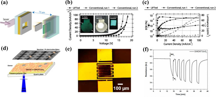
LITI can pattern multilayer architectures to fabricate OLEDs on a huge-size mother glass. The performances of printed OLED devices were proved to be high enough for commercial application [44]. A 50 nm thick alcohol-soluble polyfluorene (PFN) layer and an aluminum cathode layer can be laser - printed onto the OLED substrate to produce a polymer light-emitting diode (PLED) [27]. The LIFT printed pixel delivers competitive performance and higher efficiency in the first-run operation (Fig. 12a-c).
Fig. 12.
a Schematic illustration showing the LIFT printing process of PFN layer and Al layer onto a glass/ITO/PEDOT:PSS/PVK acceptor substrate for fabricating a polymer light-emitting diode (PLED) pixel. b Current density curves versus voltage for the PLED pixels using LIFT and conventional techniques. Insets show the digital figures of a traditional device during operation (left) and after burnout (middle) and a LIFT printed pixel during operation (right). c Curves of external quantum efficiency and luminance versus current density of devices. d The schematic illustration shows the LIFT printing process of SWCNT@SnO2 onto a glass acceptor with metal electrodes for fabricating the NH3 sensor. e Optical microscopy figures of a LIFT printed SWCNT@SnO2 pixel on the Pt electrodes. f The real-time sensing performance of the printed SWCNT@SnO2 sensor under different concentrations of NH3. a–c Reproduced from ref [27] with permission.
Copyright 2012, American Chemical Society. d–f Reproduced from ref [47] with permission. Copyright 2021, Multidisciplinary Digital Publishing Institute
High-Throughput Material Synthesis
It is possible to swiftly synthesize and characterize various materials using high-throughput and combinatorial experimentation. Printing hundreds to thousands of samples on a single printable substrate is feasible using this method. This technology can speed up new material discovery and optimization, spending only a fraction of the cost of conventional approaches. However, developing reliable printing techniques that can reproduce a wide range of materials remains a key challenge in high-throughput and combinatorial research. Obtaining usable information from high-throughput experimental data necessitates proper data processing and evaluation. Throughput and combinatorial experiments can revolutionize material discovery and optimization, despite these challenges.
Automatic solid-phase methods have greatly improved the ability to synthesize tiny and large compounds, such as oligomers and polymers. Peptide microarrays with thousands of distinct sequences can be synthesized using the LIFT system. A LIFT-based microarray synthesizer was developed to produce up to 20 residue peptides with a density of 10,000 spots per cm2 [45]. These produced peptide microarrays were used to study the IgG response in a survivor of Ebola virus sickness. Microarrays and combinatorial screening can now be carried out at much higher throughputs because of the quick chemical reactions occurring in ultrasmall quantities. Direct writing in the femtoliter range can be achieved using LIFT, a more versatile method. Polymer patches containing chemical building blocks were transferred through a new-version LIFT using low-cost diode lasers. It allows for chemical reactions in a femtoliter range for combinatorial chemistry. Irreversible deformation under laser irradiation would occur in traditional donor films (e.g., polyimide), which limits the large-scale application of LIFT. A stable hematite nanolayer was developed as a laser absorber in the donor film to achieve high-throughput femtoliter chemistry [46]. Hydrophilic polymers were transferred in femtoliter volumes using this novel laser absorber nanofilm. This method is much less expensive and more flexible than atomic force microscopy (AFM)-based scanning probe lithography.
Sensors
Sensors play a growing role in our lives, from smartphones to automobiles. Sensors monitoring temperature, humidity, pressure, and chemical signals are the fundamental building elements in intelligent devices and the Internet of Things (IoT). As most of the components of sensors can be printed, direct printing is a convenient approach to fabricating all kinds of sensors. Future printed sensors will make our lives smarter and more interconnected.
SWCNT@SnO2 nanocomposite ammonia sensors based on LIFT-printed metallic geometries were effectively constructed [47]. The assembled sensor can accurately monitor NH3 at a concentration as low as 24 ppm (Fig. 12d-f). IgG microarrays can be transferred onto a glass substrate for fabricating biosensors using LIFT [48]. LIFT was used to transfer thylakoids onto a screen-printed electrode to achieve nanomolar herbicide detection [49]. The transferred thylakoids were anchored in the porous electrode structure and showed a high photocurrent signal. The LIFT approach allowed for high-resolution printing of liquid biomaterials, making it perfect for depositing biomaterials onto the microelectrodes of sensing devices.
Photonics
The optical phenomenon of surface plasmon resonance (SPR) happens when light waves reflect off a substance. The material structure enables the waves to interact, generating a collective oscillation of electrons. This resonant oscillation can be stimulated by incident light, producing a population of energetic electrons known as surface plasmons. SPR is used in numerous applications, including material characterization, solar energy conversion, and sensors. Scientists can create new and superior materials and gadgets for various applications by comprehending and manipulating surface plasmons.
Crystalline single Ge and SiGe nanoparticles were made using a femtosecond LIFT printing process. It is possible to use these nanoparticles for photonic applications since they have dipole resonances in a wide light spectrum [22]. Metamaterials are constructed of carefully designed nano/microstructures that demonstrate exceptional optical features, such as negative refraction index. As one of the most promising methods for creating fine multilayer structures in micro- and nano-plasmonic metamaterials, laser direct writing (LDW) is an excellent choice. With femtosecond LIFT, an array of multilayer split resonant ring was created, and the reflection spectra were perfectly consistent [50].
Integrated Circuits
The material chosen for the interconnects in an integrated circuit is critical for numerous reasons. The material used in a circuit must be electrically conductive to convey signals between components. A second need is that the material can withstand the high temperatures generated during the production of an integrated circuit. Metals and dielectrics on the integrated circuit must be compatible with any material. Finally, the material must be strong enough to support the interconnect’s weight. Conductive polymers, metals (such as copper and aluminum), and carbon nanotubes were frequently used as interconnects, which all can be printed using laser-induced methods.
LIFT can print electronic devices on non-nonconventional flexible substrates such as r-paper (Fig. 10b). The inductors printed using LIFT were superior to those printed on c-paper using inkjet printing [9].
Electrochemical Catalysts
Catalysts play a critical role in efficient electrochemical systems, for instance, in water splitting. Water splitting is a promising way to obtain hydrogen energy. Catalysts can greatly improve the performance of hydrogen evolution reaction (HER) and oxygen evolution reaction (OER). The efficiency of the catalyst is determined by its active surface area. Therefore, the electrochemical catalysts are usually fabricated into nanoparticles and mixed with conductive nanocomponents (e.g., graphene nanosheets) to avoid agglomeration. Compared with traditional high-temperature methods for fabricating nano-scale electrochemical catalysts, LIFT is a more efficient approach with the advantages of large scale, room temperature, and rapid preparation. For example, a 3D graphene framework containing a library of single-atom catalysts can be fabricated using LIFT and laser carbonization (Fig. 10c).
LIFT can fabricate and transfer catalysts on hard or soft substrates simultaneously. The graphene-supported nanoparticle electrocatalysts were fabricated using LIFT [51]. The donor was a PI film with a metal coating (Pt, Ru, or Ni). Plain glass or laser-induced graphene (LIG) film was an acceptor. In the LIFT process, the metal coating and part of the PI were transformed into graphene-supported metal nanoparticles. The formed nanoparticles were ejected from the donor onto the acceptor. The fabricated catalysts supported on the acceptor film can be directly used as an integrated electrode in HER or OER without a binder. The graphene-supported Pt nanoparticles showed excellent catalytic activity in HER. The graphene-supported Ru/Ni nanoparticles can be used as OER catalysts. Bimetallic nanoparticle electrocatalysts can also be fabricated using LIFT [52]. A PI film with CuPd mixture coating was used as the donor. After the LIFT process, the graphene-supported CuPd nanoparticles were deposited on an ITO glass. The catalyst electrode has shown high activity on the glycerol oxidation with high selectivity for valuable C3 products. The catalytic performances of the sample can be optimized by adjusting the ratio of Cu and Pd in the donor film.
Perspective
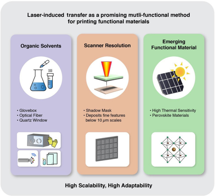
As previously discussed in this work, laser-induced transfer is a multi-functional method for printing functional materials for various applications. Their high scalability and adaptability are useful for deploying more categories of materials shortly (Fig. 13). Nevertheless, several key technical problems still restrict their industrialized applications. These include the relatively low resolution, limited heat-labile or flammable materials usage, and weak adhesion between printed materials and acceptors. Here, we propose some promising strategies to deal with these issues and promote their practical applications.
Fig. 13.
Schematic illustration of future perspectives of laser-induced printing as a promising method for printing functional materials
First, although laser scanners are fast, their writing resolution is limited, especially for low-cost scanning systems such as motor-driven plots or Galvo scanners. The resolution of laser-induced transfer printing is almost equal to the laser writing resolution. The minimum linewidth of the pattern printed through laser-induced transfer is usually greater than 10 µm. A shadow mask is an option for depositing fine dots below 10 µm diameters to enhance the laser-induced transfer resolution. The shadow mask can be installed on the upper surface of the donor, the bottom surface of the donor, or the upper surface of the acceptor to reduce the area of the irradiated spot, donated spot, or accepted spot, respectively. All these masks can make the printed dots smaller, ensuring a higher resolution. The different installed positions will have quite different effects on the microstructure of the printed dots. Otherwise, a short-wavelength pulse laser and a high-efficiency focusing system can ensure a high printing resolution.
Second, the transient ultra-high temperature generated by the pulse laser will limit the usage of heat-labile or flammable materials. For example, perovskite materials have a low thermal tolerance. Several groups have developed laser annealing processes to enhance perovskite solar cells’ performance [53]. However, to our knowledge, there is still no report using LIFT to print perovskite family materials. Using a low-melting-point dynamic release layer can help protect the perovskite donor layer under transient pulse laser heating, ensuring the LIFT printing of perovskite. After printing, the residual of the low-melting-point dynamic release layer can be easily removed by the simple heating process. Otherwise, the laser-induced transfer process can be carried out in an inert gas chamber to print flammable or organic solvent materials. For example, the laser system can be installed in a glovebox for in situ transferring. Meanwhile, the laser can be introduced into the inert gas chamber using an optical fiber or a quartz window, which can also avoid the problem of thermal dissipation in the laser system.
Lastly, the laser-induced transfer printed materials usually show poor adhesion, especially for materials with high melting points. The main reason is that most donor materials are transferred onto the acceptor in their original states. When using a solid donor layer, the laser-induced transfer printed dots are jetted onto the acceptor in the solid state. Although some melting and vaporization occurred under pulse laser irradiation, the transferred materials will be cooled down into solid in nanoseconds. Compared with the traditional fusion-based printing techniques, the laser-induced transfer method does not involve a slow nucleation process to form strong internal bonding (crystal or molecular bonding) inside the patterns. Instead, the laser-induced transfer printed dots are stacked under Van der Waals forces. Thus, the interconnection between printed patterns and the donor is weak due to the same reason. Two promising strategies are proposed to deal with this challenge. One is to use the binder to enhance the interconnection of printed patterns. The binder can be mixed with the target materials in a slurry donor layer. The solvent in printed slurry patterns will volatilize quickly, leaving a well-interconnected pattern on the acceptor. Furthermore, the binder can be post-printed onto the same location as the first printed target pattern for post-reinforcing. Another strategy is to deploy post-annealing treatment to promote the reconstruction of crystal structure in printed patterns. However, this treatment process will consume extra energy and may lead to minor structural deformation in patterns. Deploying rapid annealing or pulse-laser assisted annealing processes may help to overcome these challenges.
Conclusion
Laser-induced transfer for selectively depositing functional materials using in various applications has developed rapidly during the last few decades. With the introduction of a high-performance dynamic release layer, more novel functional materials will soon be possible to be printed through this technique. We believe this review will give materials chemistry readers a solid foundation for future study of these fascinating printing processes.
Acknowledgements
This work is funded by the Hong Kong Research Grants Council (25201620/HKUST RU449) and Hong Kong Innovation Technology Commission (ITC) under project no. MHP/060/21. The authors also acknowledge the support from the State Key Laboratory of Advanced Displays and Optoelectronics Technologies at HKUST.
Abbreviation
- ABS
Acrylonitrile butadiene styrene
- IC
Integrated circuit
- ITO
Indium tin oxide
- LIBT
Laser-induced backward transfer
- LIFT
Laser-induced forward transfer
- LITI
Laser-induced thermal imaging
- OLED
Organic light-emitting diode
- PVD
Physical vapor deposition
- SPR
Surface plasmon resonance
Data availability
No data was used for the research described in this article.
Declarations
Conflict of interest
There is no conflict of interest from the authors.
Footnotes
Publisher's Note
Springer Nature remains neutral with regard to jurisdictional claims in published maps and institutional affiliations.
References
- 1.Tillmann M, Dakić B, Heilmann R, Nolte S, Szameit A, Walther P. Nat Photonics. 2013;7:540–544. doi: 10.1038/nphoton.2013.102. [DOI] [Google Scholar]
- 2.Nieminen TA, Knöner G, Heckenberg NR, Rubinsztein-Dunlop H. Methods Cell Biol. 2007;82:207–236. doi: 10.1016/S0091-679X(06)82006-6. [DOI] [PubMed] [Google Scholar]
- 3.Hopp B, Smausz T, Kresz N, Barna N, Bor Z, Kolozsvári L, Chrisey DB, Szabó A, Nógrádi A. Tissue Eng. 2005;11:1817–1823. doi: 10.1089/ten.2005.11.1817. [DOI] [PubMed] [Google Scholar]
- 4.Santos MV, Paula KT, de Andrade MB, Gomes EM, Marques LF, Ribeiro SJL, Mendonca CR. ACS Appl Mater Interfaces. 2020;12:50033–50038. doi: 10.1021/acsami.0c13482. [DOI] [PubMed] [Google Scholar]
- 5.Papavlu AP, Mattle T, Temmel S, Lehmann U, Hintennach A, Grisel A, Wokaun A, Lippert T. Sci Rep. 2016;6:25144. doi: 10.1038/srep25144. [DOI] [PMC free article] [PubMed] [Google Scholar]
- 6.Xu D, Chan KC, Guo HJ, Zhong H, Lu L. Journal of Materials Chemistry A. 2021;9:16470–16478. doi: 10.1039/d1ta01267c. [DOI] [Google Scholar]
- 7.Feinaeugle M, Heath DJ, Mills B, Grant-Jacob JA, Mashanovich GZ, Eason RW. Appl Phys A. 2016;122:398. doi: 10.1007/s00339-016-9953-6. [DOI] [Google Scholar]
- 8.Liang P, Liu B, Wang Y, Liu KX, Zhao YP, Huang WE, Li B. Appl Environ Microbiol. 2022;88:e01165–e1221. doi: 10.1128/aem.01165-21. [DOI] [PMC free article] [PubMed] [Google Scholar]
- 9.Sopena P, Sieiro J, Fernandez-Pradas JM, Lopez-Villegas JM, Serra P. Advanced Materials Technologies. 2020;5:2000080. doi: 10.1002/admt.202000080. [DOI] [Google Scholar]
- 10.Pozov SM, Andritsos K, Theodorakos I, Georgiou E, Ioakeimidis A, Kabla A, Melamed S, De La Vega F, Zergioti I, Choulis SA. ACS Appl Electron Mater. 2022;4:2689–2698. doi: 10.1021/acsaelm.2c00217. [DOI] [PMC free article] [PubMed] [Google Scholar]
- 11.Delrot P, Hauser SP, Krizek J, Moser C. Appl Phys A. 2018;124:616. doi: 10.1007/s00339-018-2030-6. [DOI] [Google Scholar]
- 12.Duocastella M, Fernandez-Pradas JM, Dominguez J, Serra P, Morenza JL. Appl Phys A. 2008;93:941–945. doi: 10.1007/s00339-008-4741-6. [DOI] [Google Scholar]
- 13.Duocastella M, Fernandez-Pradas JM, Serra P, Morenza JL. Appl Phys A. 2008;93:453–456. doi: 10.1007/s00339-008-4781-y. [DOI] [Google Scholar]
- 14.Yung WKC, Sun B, Meng ZG, Huang JF, Jin YD, Choy HS, Cai ZX, Li GJ, Ho CL, Yang JL, Wong WY. Sci Rep. 2016;6:39584. doi: 10.1038/srep39584. [DOI] [PMC free article] [PubMed] [Google Scholar]
- 15.Zhong H, Zhu Z, You P, Lin J, Cheung CF, Lu VL, Yan F, Chan C-Y, Li G. ACS Nano. 2020;14:8846–8854. doi: 10.1021/acsnano.0c03504. [DOI] [PubMed] [Google Scholar]
- 16.Kuznetsov AI, Koch J, Chichkov BN. Opt Express. 2009;17:18820–18825. doi: 10.1364/Oe.17.018820. [DOI] [PubMed] [Google Scholar]
- 17.Logotheti A, Zacharatos F, Makrygianni M, Zergioti I. Appl Surf Sci. 2020;512:145730. doi: 10.1016/j.apsusc.2020.145730. [DOI] [Google Scholar]
- 18.Zywietz U, Evlyukhin AB, Reinhardt C, Chichkov BN. Nat Commun. 2014;5:3402. doi: 10.1038/ncomms4402. [DOI] [PubMed] [Google Scholar]
- 19.Gorodesky N, Sedghani-Cohen S, Altman M, Fogel O, Cohen-Taguri G, Fleger Y, Kotler Z, Zalevsky Z. Adv Func Mater. 2020;30:2001260. doi: 10.1002/adfm.202001260. [DOI] [Google Scholar]
- 20.Gorodesky N, Sedghani-Cohen S, Fogel O, Altman M, Cohen-Taguri G, Kotler Z, Zalevsky Z. Adv Eng Mater. 2022;24:2100952. doi: 10.1002/adem.202100952. [DOI] [Google Scholar]
- 21.Sammartino C, Cohen SS, Kotler Z, Eliaz N. Adv Eng Mater. 2021;23:2100245. doi: 10.1002/adem.202100245. [DOI] [Google Scholar]
- 22.Zhigunov DM, Evlyukhin AB, Shalin AS, Zywietz U, Chichkov BN. ACS Photonics. 2018;5:977–983. doi: 10.1021/acsphotonics.7b01275. [DOI] [Google Scholar]
- 23.Heidmann B, Andree S, Levcenko S, Unold T, Abou-Ras D, Schafer N, Bonse J, Kruger J, Schmid M. Acs Appl Energy Mater. 2018;1:27–31. doi: 10.1021/acsaem.7b00028. [DOI] [Google Scholar]
- 24.Shaw-Stewart J, Lippert T, Nagel M, Nuesch F, Wokaun A. ACS Appl Mater Interf. 2011;3:309–316. doi: 10.1021/am100943f. [DOI] [PubMed] [Google Scholar]
- 25.Theodorakos I, Kalaitzis A, Makrygianni M, Hatziapostolou A, Kabla A, Melamed S, de la Vega F, Zergioti I. Adv Eng Mater. 2019;21:1900605. doi: 10.1002/adem.201900605. [DOI] [Google Scholar]
- 26.Makrygianni M, Milionis A, Kryou C, Trantakis I, Poulikakos D, Zergioti I. Adv Mater Interf. 2018;5:1800440. doi: 10.1002/admi.201800440. [DOI] [Google Scholar]
- 27.Shaw-Stewart JRH, Lippert TK, Nagel M, Nuesch FA, Wokaun A. ACS Appl Mater Interf. 2012;4:3535–3541. doi: 10.1021/am300598h. [DOI] [PubMed] [Google Scholar]
- 28.Lin J, Peng ZW, Liu YY, Ruiz-Zepeda F, Ye RQ, Samuel ELG, Yacaman MJ, Yakobson BI, Tour JM. Nat Commun. 2014;5:5714. doi: 10.1038/ncomms6714. [DOI] [PMC free article] [PubMed] [Google Scholar]
- 29.Li G, Mo X, Law W-C, Chan KC. J Mater Chem A. 2019;7:4055–4062. doi: 10.1039/c8ta11121a. [DOI] [Google Scholar]
- 30.Li G, Mo X, Wang Y, Chan C-Y, Chan KC. Adv Mater Interf. 2019;6:1900874. doi: 10.1002/admi.201900874. [DOI] [Google Scholar]
- 31.Jiang N, Wang Y, Chan KC, Chan C-Y, Sun H, Li G. Global Chall. 2020;4:1900054. doi: 10.1002/gch2.201900054. [DOI] [PMC free article] [PubMed] [Google Scholar]
- 32.Wang Y, Li G, Chan KC. Solar Energy Mater Solar Cells. 2020;218:110693. doi: 10.1016/j.solmat.2020.110693. [DOI] [Google Scholar]
- 33.Zhong H, Zhu Z, Lin J, Cheung CF, Lu VL, Yan F, Chan C-Y, Li G. ACS Nano. 2020;14:6213–6221. doi: 10.1021/acsnano.0c02250. [DOI] [PubMed] [Google Scholar]
- 34.Lou KY, Qian J, Yu XH, Xia ZY, Shen DY, Wang GD, Zhao QZ. Adv Mater Interf. 2022;9:2102347. doi: 10.1002/admi.202102347. [DOI] [Google Scholar]
- 35.Lou KY, Qian J, Yu XH, Xia ZY, Shen DY, Wang GD, Zhao QZ. Chin Opt Lett. 2022;20:043801. doi: 10.3788/Col202220.043801. [DOI] [Google Scholar]
- 36.Lin J, Zhu Z, Cheung CF, Yan F, Li G. J Mater Chem C. 2020;8:10587–10603. doi: 10.1039/D0TC01112F. [DOI] [Google Scholar]
- 37.Li G, Law W-C, Chan KC. Green Chem. 2018;20:3689–3695. doi: 10.1039/c8gc01347k. [DOI] [Google Scholar]
- 38.Huang LB, Ling L, Su JJ, Song Y, Wang ZY, Tang BZ, Westerhoff P, Ye RQ. ACS Appl Mater Interf. 2020;12:51864–51872. doi: 10.1021/acsami.0c16596. [DOI] [PubMed] [Google Scholar]
- 39.Colina M, Morales-Vilches A, Voz C, Martín I, Ortega P, Orpella A, López G, Alcubilla R. Appl Surf Sci. 2015;336:89–95. doi: 10.1016/j.apsusc.2014.09.172. [DOI] [Google Scholar]
- 40.Chen Y, Munoz-Martin D, Morales M, Molpeceres C, Sanchez-Cortezon E, Murillo-Gutierrez J. Phys Procedia. 2016;83:204–210. doi: 10.1016/j.phpro.2016.08.010. [DOI] [Google Scholar]
- 41.Munoz-Martin D, Brasz CF, Chen Y, Morales M, Arnold CB, Molpeceres C. Appl Surf Sci. 2016;366:389–396. doi: 10.1016/j.apsusc.2016.01.029. [DOI] [Google Scholar]
- 42.Kandyla M, Chatzandroulis S, Zergioti I. Opto-Electron Rev. 2010;18:345–351. doi: 10.2478/s11772-010-0045-4. [DOI] [Google Scholar]
- 43.Yung WKC, Sun B, Huang J, Jin Y, Meng Z, Choy HS, Cai Z, Li G, Ho CL, Yang J, Wong WY. Sci Rep. 2016;6:31188. doi: 10.1038/srep31188. [DOI] [PMC free article] [PubMed] [Google Scholar]
- 44.Wolk MB, Lamansky S, Tolbert WA. SID Symp Digest Tech Papers. 2008;39:511. doi: 10.1889/1.3069713. [DOI] [Google Scholar]
- 45.Paris G, Heidepriem J, Tsouka A, Liu YX, Mattes DS, Martin SP, Dallabernardina P, Mende M, Lindner C, Wawrzinek R, Rademacher C, Seeberger PH, Breitling F, Bischoff FR, Wolf T, Loeffler FF. Adv Mater. 2022;34:2200359. doi: 10.1002/adma.202200359. [DOI] [PubMed] [Google Scholar]
- 46.Zhang JF, Liu YX, Ronneberger S, Tarakina NV, Merbouh N, Loeffler FF. Adv Mater. 2022;34:2108493. doi: 10.1002/adma.202108493. [DOI] [PubMed] [Google Scholar]
- 47.Bonciu AF, Filipescu M, Voicu SI, Lippert T, Palla-Papavlu A. Nanomaterials. 2021;11:2604. doi: 10.3390/nano11102604. [DOI] [PMC free article] [PubMed] [Google Scholar]
- 48.Duocastella M, Fernandez-Pradas JM, Serra P, Morenza JL. J Laser Micro Nanoeng. 2008;3:1–4. doi: 10.2961/jlmn.2008.01.0001. [DOI] [Google Scholar]
- 49.Touloupakis E, Boutopoulos C, Buonasera K, Zergioti I, Giardi MT. Anal Bioanal Chem. 2012;402:3237–3244. doi: 10.1007/s00216-012-5771-7. [DOI] [PubMed] [Google Scholar]
- 50.Tseng ML, Wu PC, Sun SL, Chang CM, Chen WT, Chu CH, Chen PL, Zhou L, Huang DW, Yen TJ, Tsai DP. Laser Photonics Rev. 2012;6:702–707. doi: 10.1002/lpor.201200029. [DOI] [Google Scholar]
- 51.Mo X, Chan KC, Tse ECM. Chem Mater. 2019;31:8230–8238. doi: 10.1021/acs.chemmater.9b03669. [DOI] [Google Scholar]
- 52.Mo X, Gao X, Gillado AV, Chen H-Y, Chen Y, Guo Z, Wu H-L, Tse ECM. Direct 3D printing of binder-free bimetallic nanomaterials as integrated electrodes for glycerol oxidation with high selectivity for valuable C3 products. ACS Nano. 2022;16:12202–12213. doi: 10.1021/acsnano.2c02865. [DOI] [PubMed] [Google Scholar]
- 53.You P, Li G, Tang G, Cao J, Yan F. Energy Environ Sci. 2020;13:1187–1196. doi: 10.1039/C9EE02324K. [DOI] [Google Scholar]
Associated Data
This section collects any data citations, data availability statements, or supplementary materials included in this article.
Data Availability Statement
No data was used for the research described in this article.


