

Abstract

Simulating the plasmonic properties of colloidally derived metal nanoparticles with accuracy to their experimentally observed measurements is challenging due to the many structural and compositional parameters that influence their scattering and absorption properties. Correlation between single nanoparticle scattering measurements and simulated spectra emphasize these strong structural and compositional relationships, providing insight into the design of plasmonic nanoparticles. This Perspective builds from this history to highlight how the structural features of models used in simulation methods such as those based on the Finite-Difference Time-Domain (FDTD) method and Discrete Dipole Approximation (DDA) are of critical consideration for correlation with experiment and ultimately prediction of new nanoparticle properties. High-level characterizations such as electron tomography are discussed as ways to advance the accuracy of models used in such simulations, allowing the plasmonic properties of structurally complex nanoparticles to be better understood. However, we also note that the field is far from bringing experiment and simulation into agreement for plasmonic nanoparticles with complex compositions, reflecting analytical challenges that inhibit accurate model generation. Potential directions for addressing these challenges are also presented.
Keywords: FDTD, DDA, plasmonic, nanoparticle, simulation, modeling, tomography
Introduction
Nanoscale materials have properties that differ from their bulk counterparts, giving them applications in sensing, catalysis, medicine, and more.1−8 Optically active nanomaterials have been used in stained glass since ancient Rome, with the famous Lycurgus cup as a beautiful example where the apparent color of the cup given by the nanoparticles embedded within the glass depends on the location of the light source. Colloidal metal nanoparticles have attracted much interest for their widely tunable properties that are accessible from scalable, bottom-up approaches.9−14 Many colloidal syntheses produce metal nanoparticles of high symmetry; however, nanoparticles with structural and compositional complexity can also be obtained. For example, Au nanostars are useful plasmonic nanoparticles for biomedical applications but lack defined symmetry, and multimetallic nanoparticles are of increasing importance to applications such as catalysis.5,15−19 Moreover, colloidal syntheses of metal nanoparticles produce samples with inherent heterogeneity; i.e., slight structural variations from one nanoparticle to the next in a sample.20 As will be outlined herein, this complexity of nanoparticle samples often necessitates corroboration of their nanoscale properties with simulation.
Nanoparticle features such as particle size, shape, composition, and architecture can be manipulated through colloidal syntheses. In turn, these features influence the localized surface plasmon resonances (LSPRs) of a metal nanoparticle. An LSPR is a collective oscillation of the conduction electrons of a nanoparticle induced by incident light. The energy of this resonance depends on the structure, composition, and surrounding environment of the nanoparticle, highlighting the attractiveness of colloidal syntheses but also the need to accurately capture these qualities in any simulation.1 Gustav Mie analytically solved Maxwell’s equations for the scattering properties of an electromagnetic plane wave from a homogeneous sphere in 1908.21 Systematic studies have subsequently shown excellent correlation between experimentally measured and analytically derived optical properties, highlighting how representative models of simple convex shapes were relatively straightforward to construct.22−26 However, the Mie solution is limited to simple structures such as spheres and cylinders.21
For more complex shapes, the finite-difference time-domain (FDTD) method—a numerical modeling tool for electrodynamics—is appropriate. Originally published by Yee in 1966, FDTD discretizes 3D space into compartments known as Yee cells across which Maxwell’s equations may be solved.27 After the simulation has been broken down into a 3D grid, the electric and magnetic field components are then sequentially and recursively updated as they propagate across the mesh in defined time steps. The interaction of the electronic and magnetic field components is then recorded for interpretation. The implementation of the FDTD method has historically been limited by the required computational resources but has become more generally available as those costs have decreased.28 The FDTD method is now widely used due to its simple implementation and generality to many systems. However, the meshing size of the Yee cells may result in discontinuities from staircasing curved surfaces to a Euclidean grid.28−31 This staircasing effect can be reduced by discretizing the 3D space to arbitrary precision, but the resources required then to process the simulation increase with mesh step size.28
In this Perspective, practical considerations for simulations of metal nanoparticles are discussed, such as this staircasing effect, with particular emphasis on bringing simulation and experiment into agreement for structurally and compositionally complex nanoparticles. We begin by highlighting select ground-breaking single-particle correlation studies that give insight into the importance of realistic nanoparticle models for FDTD and DDA simulations. Like FDTD, the DDA method is used to compute the scattering of light by particles of arbitrary size and shape, where in this case the particle is approximated as an array of dipoles that interact with the light and each other.32,33 We then discuss practical considerations when creating models for such simulations by showing the spectral changes that arise from subtle changes to a given model or simulation parameter. These considerations lay the foundation for the emerging interest in using tomographical reconstructions to create accurate models for simulation, which is proving quite useful to the field of chiroptical nanomaterials. We note that the examples presented here are not comprehensive but were selected to illustrate the main conceptual approaches toward high-quality model generation. We conclude with challenges to the field in accurately capturing nanomaterials with complex compositions for simulations.
Correlative Single-Particle Studies
Analyzing the relationship between particle structure and its optical properties is fundamentally difficult due to the inherent heterogeneity of NP samples, where commonly ensemble responses are measured and an assumption is made that the average structure observed accounts for the response.34,35 Yet, there is evidence that this assumption is a poor one. For example, in the seminal 1997 paper on single-molecule and single-nanoparticle surface-enhanced Raman scattering (SERS), Nie and Emory posited that the bulk of the Raman signal originated from less than 1% of the nanoparticles in the population, suggesting that the enhancement associated with this subpopulation was 106–107 higher than the ensemble averaged value.36 Single-particle studies can address the effects of heterogeneity from one NP to the next. For example, correlative studies can be undertaken in which the scattering properties of single NPs are measured alongside high-level structural characterization by electron microscopy.34,37 Such approaches allow for fine structural information to be correlated to the optical properties of specific NPs. In turn, structure–property trends can be established, and NPs with outlier properties can be identified.
The importance of fine structural features to the plasmonic properties of metal NPs was particularly evident for a systematic study by Van Duyne and co-workers, where the optical responses of individual Au and Ag nanocubes were measured by dark-field scattering spectroscopy and these results were correlated to structural features from high-resolution transmission electron microscopy (TEM) images.37 To bring the experimentally obtained scattering spectra into agreement with FDTD simulations, the models needed to accurately capture the subtle structural features of the Au and Ag nanocubes. That is, the simplest models of platonic solids have perfectly defined edges and vertices, but as the TEM image of a Ag nanocube shows (Figure 1A), atomically sharp corners and edges are not observed. Instead, rounded corners are evident.
Figure 1.
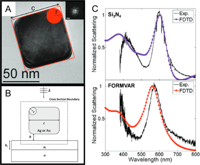
(A) TEM image of an individual Ag nanocube (inset electron diffraction pattern along the [100] direction), where c defines the face-to-face distance and r defines the radius of curvature. (B) Representative structural model of a nanocube with these structural features as well as the underlying substrate, with the cube positioned at a distance h from the substrate. Substrate with thickness hl and refractive index nl atop an infinite glass surface with refractive index n = 1.5. (C) Simulated (purple and red traces) and experimental scattering spectra (black traces) for single Au nanocubes on Si3N4 (top) and Formvar (bottom). Au nanocube dimensions are (c = 74.2 nm, r = 12.7 nm) and (c = 84.0 nm, r = 15.2 nm) on the Si3N4 and Formvar substrates, respectively. Reproduced with permission from ref (37). Copyright 2010 American Chemical Society.
The models developed by Van Duyne and co-workers for Au and Ag nanocubes captured the fine structural features observed by TEM by including face-to-face distance (c) and the radius of curvature (r) of isolated nanocubes (Figure 1B). However, this model was insufficient to accurately bring experiment and simulation in agreement. The dielectric environment surrounding the NPs had to be accurately captured, meaning that the substrate supporting the NPs and its distance from the NPs must be included in the model. Unfortunately, measuring the distance between the nanocubes and substrate is experimentally challenging. To gain insight into this feature, the optical response of Au nanocubes was systematically studied as a function of position and substrate identity by simulation, where a substrate of thickness hl, nl refractive index, and h distance away from the nanocube was added to the simulation (Figure 1B). As shown in Figure 1C, good agreement between simulation and experiment was achieved when the structural features of the Au nanocubes were included in conjunction with the substrate (either Si3N4 or Formvar), with the Au nanocubes positioned at the surface. Van Duyne and co-workers did note a few subtle discrepancies in terms of peak width and peak dips and readers are referred to the original reference for the excellent in-depth discussion.37 For our purposes, however, this systematic study shows quite well how important the fine features of models are to bring simulation and experiment into agreement.
These same ideas hold when moving to metal nanoparticles of other shapes. For example, Van Duyne and co-workers also studied the plasmonic properties of single Ag triangular nanoprisms by dark-field optical microscopy and spectroscopy, bringing agreement between experiment and electrodynamic modeling based on the DDA method.34 This agreement was achieved through careful consideration of nanoprism height, edge length, and tip sharpness. This study was particularly impactful for showing how simulation can be applied to polydisperse nanoparticle samples, especially when coupled with single-particle approaches. That is, nanoparticle samples with large polydispersity will give rise to broad LSPRs as each nanoparticle in the sample has a slightly different spectrum that contributes to the ensemble response. This feature is evident in Figure 2A, where the black curve corresponds to the ensemble spectrum of the triangular Ag nanoprisms, while the scattering spectra from single Ag nanoprisms are much narrower as denoted by the colored curves, spanning a λmax of ∼600 to 700 nm depending on the edge length (Figure 2A). Notably, the scattering spectra of the single triangular nanoprisms fall within the envelope of the ensemble spectrum. Moreover, good agreement was achieved between simulation and experiment as shown in Figure 2B, where the model for simulations based on the DDA method was created from dimensions extracted from atomic force microscopy.
Figure 2.
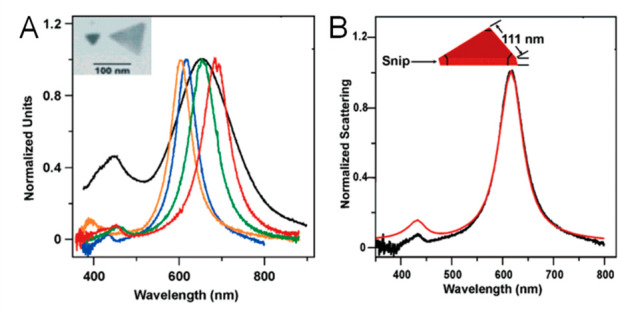
(A) Ensemble (black trace) and individual scattering spectra (color traces) for triangular Ag nanoprisms. TEM image in inset. (B) Simulated (red trace) and experimental scattering spectrum (black trace) for a single Ag nanoprism, with model included as inset. Reproduced with permission from ref (34). Copyright 2006 American Chemical Society.
Many studies report correlation between nanoparticle structures with their observed optical properties through simulation.26,38−46 These examples highlight how simulations can address complex samples with heterogeneity, providing relevant structure–property relationships. Significantly, the structural features of nanoscale systems must be accurately captured in models for sufficient correlation with experimental data.
Structural Considerations for Models in FDTD Simulations
Simulations of single-particle scattering spectra highlight the sensitivity of their λmax to slight structural perturbations. In this section, we raise awareness of the structural considerations for models used in FDTD simulations. Toward this end, we created a structural model of a Au nanocube similar to Van Duyne and co-workers, with the corners and edges are defined by a radius of curvature r and face-to-face distance c (Figure 1A).37 However, the refractive index of the medium was set at 1.333 (no substrate) to mimic colloidal measurements in water; the simulation mesh was set to 2 nm. The face-to-face distance and radius of curvature were systematically changed to investigate changes in λmax. Finally, the dielectric information reported by Johnson and Christy for bulk Au is used for the nanocube material.47 The dielectric information was measured by ellipsometry on thin films, but this information may also be measured by electron energy loss spectroscopy (EELS) and X-ray photoelectron spectroscopy (XPS).48,49 We note, however, that measured dielectric properties may vary from theory due to inter- and intraband transitions unique from free-electron contributions.50−54 We further acknowledge that there are deviations from the measured true dielectric function when approximated by a polynomial expression for FDTD; however, there is historically good agreement between experimental and numerical optical properties suggesting that the approximation sufficiently represents the dielectric behavior at least for many simple compositions.
Figure 3A shows models of the Au nanocubes used in simulations, where c = 100 nm and r was varied from 0 to 40 nm in steps of 10 nm. The resulting scattering spectra are shown in Figure 3B, where a blue shift in λmax from ∼660 nm to ∼600 nm is evident from r = 0 to 40 nm. This blue shift is consistent with the work by Van Duyne and co-workers and highlights how models for FDTD simulations should incorporate realistic facet truncations to achieve experimentally realistic positions in λmax.37 We observed that the edge length, the distance between vertices on the cube, decreases with increasing rounding. Thus, an additional rounded model with edge length of 100 nm was created as well to compare rounding and face-to-face distance with edge length directly. We observe that although the rounding causes broadening of the scattering spectrum, the simulated λmax of both the unrounded and 100 nm edge length cubes are roughly equal (Figure 3A,B). Regardless, simulations of this nature can be quite useful for revealing trends in λmax with systematic changes in structure, aiding in plasmonic nanocrystal design.
Figure 3.

Sensitivity of Au nanoparticle scattering spectra to simulation parameters. (A) Au cube models of various radii of curvature with the same face-to-face distance. One model with edge length 100 and 20 nm radius of curvature shown above. (B) Simulated scattering spectra of the Au nanocube models. (C) Au cube model with 150 nm face-to-face distance and 60 nm radius of curvature shown with representative meshing size relative to the model. (D) Simulated scattering spectra of the 150 nm face-to-face distance Au nanocube model under 2, 4, and 8 nm simulation meshes. (E) Tomographic reconstructions obtained from a single tetrahedrally seeded chiral Au nanocrystal shown from [100], [111], and [110] directions (left to right). (F) Simulated chiral g-factor spectra of the tomographic reconstruction at different orientations (color traces), and the average of all orientations (black). (E, F) Reprinted with permission under a Creative Commons CC-BY License from ref (59). Published 2022 Royal Society of Chemistry.
Still, for such trends to be successfully extracted, the simulation parameters must be carefully selected to avoid undesirable staircasing effects. Selecting the mesh size is of critical importance with the FDTD method, with structures with fine structural features (e.g., sharp corners) necessitating smaller mesh sizes than large structural features. While decreasing the mesh size generally decreases the accumulated error, the computational resources required increase.
To illustrate the effect of mesh size, we performed simulations on a model nanocube system (c = 150 nm and r = 60 nm) with mesh sizes of 2, 4, and 8 nm step length (Figure 3C). The scattering spectra are shown in Figure 3D, with the effect of improper meshing particularly evident in the spectra obtained with 4 and 8 nm step lengths. With the larger step lengths, multiple peaks appear in the spectra that are inconsistent with the symmetry of the nanocube as well as experimental observations.55−57 These results highlight how those conducting such simulations must strike a reasonable balance between mesh size and computational time, where ensuring that the results make physical sense is essential.
Finally, one must also be cognizant of the direction of light propagation when designing simulations and its effect on the results. The scattering properties of nanoparticles are orientation dependent, so the direction of light propagation must be considered for structures of low symmetry.55,58 That is, rotation of the model in 3D space is necessary to achieve an accurate average of the scattering properties. This effect is illustrated well by considering the simulation of intrinsically chiral Au nanocrystals such as those grown from tetrahedral seeds shown in Figure 3E; these nanocrystals consist of two flattened ellipsoids stacked on top of each other but offset by 90°.59 For brevity, these chiral nanocrystals will be referred to in this text as tetrahedral-seeded chiral Au nanocrystals. In Figure 3F are the simulated scattering spectra of the tetrahedral-seeded chiral Au nanocrystals, where each color trace corresponds with a g-factor spectrum from a different orientation. Notably, the simulated chiroptical behavior of this nanocrystal changes significantly with orientation although the average spectrum (black trace) agrees well with the experimentally measured response for these nanocrystals in solution. If a single orientation were taken instead, the chiral scattering properties would be inaccurate and, in some cases, a nearly complete inversion.
Tomography as a Tool toward Accurate Structural Modeling
As the previous section illustrated, modeling and simulation of relatively simple structures such as cubes and spheres are both fairly straightforward with high-quality microscopy imaging. This ability is aided by the high symmetry of such structures. However, the previous section also showed the sensitivity of accurate simulation to fine structural features, which can become difficult to accurately capture in complex nanoparticles of lower symmetry compared to, for example, cubes or spheres. Robust methods for model generation are required.
One method that has been leveraged to gain fine 3D structural information for complex nanocrystals is focused ion beam (FIB) milling for SEM imaging. FIB SEM enables acquisition of cross-sectional images that can reveal internal or sandwiched features of a nanoparticle, which can be directly incorporated or compiled together as a slice-wise structural model. For example, Lee et al. detailed the synthesis of intrinsically chiral Au nanocrystals through reduction of HAuCl4 onto Au seeds, where the chirality was induced by chiral capping molecules during growth.60 The structure of 432 helicoid III was probed by FIB helium ion milling coupled with SEM imaging as shown in Figure 4A. By gently ablating several nanocrystals, sequential cross-sectional SEM images were captured. From these images, the 3D nature of the chiral gaps within the nanocrystals could be more realistically understood as denoted by the red, green, and blue traces in Figures 4B–D and used to create a model for FDTD simulations (Figure 4C). Figure 4D shows the 3D interpolation of the curved surface based on the depth and curvature information obtained through FIB SEM analysis. The FDTD simulations corroborate the experimentally measured chiroptical activity of 432 helicoid III. Although the technique itself is quite sophisticated and the resulting model still idealized, FIB SEM imaging was essential to capturing the chiral gap features and bringing experiment and simulation into alignment.
Figure 4.

(A) SEM images of FIB helium ion milling on 432 helicoid III. (B) Single chiral nanoparticle highlighting the gap curvature measured from FIB SEM studies with representative models of a (C) whole nanocrystal and (D) single gap. (A–D) Reproduced with permission from ref (60). Copyright 2018 Springer Nature. (E–G) Reconstructions of Au nanostars obtained using fast in situ electron tomography after being annealed at 300 °C for 0, 30, and 1200 s, respectively. The calculated average induced electric field is shown for each reconstruction at a specified wavelength with the excitation source polarized along the most prominent tip protrusion as shown in the bottom right below each nanostar reconstruction. The scale of enhancement is shown to the right. (H) Numerically calculated extinction cross sections for Au nanostar tomograms obtained after 0 s (black trace), 30 s (red trace), and 1200 s (blue trace). (E–H) Adapted with permission under a Creative Commons CC-BY License from ref (70). Published 2018 Royal Society of Chemistry. (I) Experimentally measured g-factor (red trace) and extinction spectrum (black trace) of tetrahedral-seeded chiral nanocrystals. (J) Numerically calculated g-factor (red trace) and scattering spectra (black trace) of the representative tomogram shown in Figure 3E. (I, J) Reprinted with permission under a Creative Commons CC-BY License from ref (59). Published 2022 Royal Society of Chemistry.
Unfortunately, FIB SEM is a destructive method, meaning that other analyses cannot be readily coupled with the high level of structural information captured. In contrast, electron tomography is a nondestructive quantitative method that can produce 3D reconstructions of nanoparticles through acquisition of scanning transmission electron microscopy (STEM) images at stepwise angles. Materials must be supported on a TEM grid and rotated through a wide range of angles for full 3D information.61−71 Thus, the technique is well-suited for nanoparticles that are simply dropcast on a grid but can be challenging for larger materials and those on substrates. The reconstruction with high shape accuracy is generated by importing these projections (i.e., images obtained at specific angles) into a processing algorithm, where we encourage the reader to read work by Jenkinson et al. for an in-depth discussion.65 An advantage of this method over FIB milling coupled with SEM imaging is the ability to generate models without introducing bias during data analysis through the destructive nature of FIB SEM itself. This advantage is particularly evident when the fine structural features of a nanocrystal cannot be inferred.
Nondestructive analytical methods are particularly important to observe morphological and optical changes of single nanoparticles over time. Tomography is well-equipped to analyze polydisperse samples and complex shapes such as Au nanostars.72 Vanrompay et al. reported the synthesis and annealing of Au nanostars, measuring morphological changes by fast in situ electron tomography as shown in Figure 4E–H.70 Contrasting with traditional tomography which may take up to an hour in acquisition time, fast in situ tomography may be conducted in as few as 6 min. The small acquisition time of fast in situ tomography lowered the effect of the electron beam, which has been shown to affect the thermal stability of otherwise beam-insensitive materials.73 Therefore, the Au nanostars were able to be heated for a given time, cooled to room temperature, and reconstructed using electron tomography to observe gradual morphological changes due to thermal annealing. The tomographic reconstructions after annealing at 300 °C for 0, 30, and 1200 s are shown in Figure 4E–G, respectively. These reconstructions were then used as models to evaluate the effect of annealing time on the extinction cross-section of the Au nanostars by the boundary element method (BEM) of optical simulation. BEM differs from previously discussed methods as only the fields on a surface are discretized, allowing greater scalability when compared to volume element based methods.74 The simulated extinction spectra are shown in Figure 4H at 0 s (black trace), 30 s (red trace), and 1200 s (blue trace). As the nanostar shape became more rounded, the electric field enhancement of the nanostar greatly decreased and discrete LSPR bands coalesced into a broad extinction spectrum. Note that the magnitude of the calculated electric field enhancement is not consistent across all reconstructions in Figure 4E–G, decreasing with the thermal annealing time. This change is consistent with a decrease in tip sharpness and highlights the importance of accurately representing the radius of curvature for a nanostar’s tips in near-field simulations for analysis of SERS measurements. Electron tomography is therefore a powerful tool to correlate nuanced structural features to optical properties when coupled with simulation.
A similar approach was used to shed insight into the tetrahedral-seeded chiral Au nanocrystals shown in Figure 3E; this model was created through tomographic reconstruction using high angle annular dark field (HAADF) scanning transmission electron microscopy (STEM).59 This level of characterization was essential as, from SEM images, we were unable to unequivocally define the intrinsic chirality that accounted for their chiroptical activity shown in Figure 4I (red trace), along with their extinction properties (black trace). However, this tomographically generated model was used in FDTD simulations, and by averaging over the various orientations as discussed in the previous section, good agreement between experiment and simulation was possible (Figure 4I versus Figure 4J).59 We particularly found this approach beneficial as there is also a need to untangle the chiroptical activity from near-field enhancement emanating from surface-bound chiral growth molecules.59 We anticipate that the application of tomographic reconstructions to create models for simulations will prove useful in many complex nanoparticle systems as shown similarly for Au nanostars, chiral Au nanorods, and chiral nanoparticle assemblies.70,72,75,76
Challenge to the Field: Accurate Compositional Information in Structural Models
Single-particle correlations between experimentally obtained scattering spectra and simulation have highlighted the value of high-resolution models and have been used to extract many meaningful structure–property trends for monometallic nanoparticles. As structurally complex systems are now being handled with advanced characterization, the next challenge for the field will be accurately modeling nanoscale systems comprised of multiple elements. Multielement nanoparticles are selected to obtain synergistic effects and new properties altogether.77,78 However, the spatial arrangement of the different elements impacts the resultant properties. For example, Woessner et al. showed that the spatial distribution of Pd within/on branched Au nanoparticles with Oh symmetry impacts their sensitivity to changes in refractive index.79 In this study, Pd-tipped octopods were compared to core@shell Au@Pd octopods and alloy AuPd octopods. Interestingly, capturing the alloy composition accurately in FDTD simulations was challenging.
Alloys are difficult to model due to a lack of data on the dielectric function of the material as well as insufficient analytical tools to adequately capture the distribution with atomic level precision. These challenges are captured well in a report by Schaak and co-workers in their study of plasmonic alloy Au1–xCux (x = 0 to 0.5) nanoparticles of quasi-spherical shape.80 The composition (Au:Cu ratio) of their colloidally prepared nanoparticles was extracted from the position of X-ray diffraction (XRD) reflections in accordance with Vegard’s law. Energy dispersive X-ray spectroscopy (EDS) was also used to determine the Au:Cu ratio. With this information as input, linear mixing was used to approximate the dielectric function of the alloy nanoparticles for simulation of the plasmon resonance frequencies by Mie theory. These results were compared to each sample’s spectrum determined by UV–visible spectroscopy. Discrepancies between the theoretically predicted plasmon resonance frequencies and those observed through experiment demonstrated that a mere linear combination of dielectric functions does not accurately reflect the composite dielectric function of these alloys.
The origin of the discrepancies was not fully elucidated and has been reported in other systems as well.22 Work by our group in collaboration with the Dragnea group highlights additional challenges to accurately capturing nanoparticles with complex compositions. Specifically, a single-particle correlation study was undertaken in which stellated Au–Pd nanocrystals with Oh symmetry were analyzed by optical dark-field spectroscopy and SEM.81 The optical dark-field spectroscopy provided the λmax of each nanocrystal analyzed and SEM was used to obtain structural information (face diagonal and tip width of the stellated nanocrystals). Contour plots of LSPR λmax as a function of tip width and face diagonal as well as resonance width and face diagonal were obtained and compared to simulated data for stellated Au-only nanocrystals with the same structural features. Differences were evident from this comparison, revealing the impact of the complex Au–Pd distribution in these nanocrystals on their plasmonic properties. In fact, this analysis was consistent with the Au–Pd nanocrystals having Pd-rich tips, which was supported by single-particle elemental mapping by STEM-EDS.81,82
Still, we caution that EDS mapping measurements represent the 3D elemental composition as a 2D projection, which means that assumptions may be made with regards to elemental distribution when trying to use such data to create models for accurate modeling.83 Toward accurate spatial distributions of complex compositions, atom probe tomography (APT) is state-of-the-art.84−86 APT features resolution of subnanometer composition regardless of atomic number, although distinction between elements of similar atomic mass is difficult. In APT, a sharp sample is put under high voltage, causing a large electrostatic field at the tip. The atoms at the tip surface are then ionized and desorbed toward the ion detector. Position-sensitive detectors may be used to measure the image projections of the tip which change with composition. Field evaporation simulations calculate the trajectories of ions to determine the 2D projection on the detector.87 These simulations can account for aberrations such as changes in tip shape that impact the surface electric field often by combining high level simulation approaches. These simulations are then used to reconstruct the tip from the projection data. The accurate elemental reconstructions highlight the utility of APT to gain 3D compositional information; however, this method requires the samples to be sharply pointed and is restricted to a 150 nm field of view. Although nanoparticles may easily fit in this size constraint, reconstruction artifacts generated by differing evaporation fields of materials generally produce undesirable structural and compositional distortions leading to poorer spatial and morphological resolution when compared to other tomographic methods. Therefore, APT is often coupled with other methods to characterize the structure separately from the elemental composition.
An example of a reconstruction from APT is shown in Figure 5A,B for complementary metal-oxide-semiconductor (CMOS) transistors, which are prominently used to manufacture integrated circuit technologies. 3D geometries of CMOS transistors display lower current leakage through tunneling effects and are therefore more desirable than their 2D planar counterparts. The example shown is in gate-all-around (Figure 5A) and trigate (Figure 5B) configurations, in which the silicon nanowire is surrounded by a gate material on all sides or three sides, respectively.85 The efficacy and electronic behavior of these structures are greatly influenced by the spatial elemental distribution, corresponding to dopant concentration and surface roughness. APT reconstructions performed on the materials accurately confirmed the elemental composition of both transistor types although the morphological distortions are present.
Figure 5.

(A) APT visualization of a gate-all-around semiconductor material. (B) APT visualization of a trigate semiconductor material. (A, B) Reproduced with permission from ref (85). Copyright 2014 Elsevier. (C) HAADF-STEM image of Au@Ag nanorod showing Z-contrast between Au core (bright) and Ag shell (darker). (D) Elemental tomogram of a Au@Ag nanorod obtained using Z-contrast to inform elemental identity. (C, D) Reproduced with permission from ref (66). Copyright 2013 American Chemical Society. (E, F) 3D elemental tomograms of hollow bimetallic Ag–Au nanoparticles created coupling STEM tomography with EDS data. (E) Ag–Au nanoparticle with low Au loading displaying high surface expression of Au. (F) Ag–Au nanoparticle with greater Au composition displaying high surface expression of Ag. (E, F) Reprinted with permission under a Creative Commons CC-BY License from ref (91). Published 2014 American Chemical Society.
Although APT can theoretically achieve atomic-scale elemental resolution, morphological distortions limit its utility for structure-dependent plasmonic simulation. Therefore, measurement of composition while also maintaining the structural information is advantageous. Toward this end, 3D tomograms with high spatial accuracy may be obtained by HAADF-STEM. HAADF-STEM imaging may then be coupled with either Z-contrast or EDS information to provide 3D elemental composition. This capability is growing with the advent of new detection capabilities for acquiring quantitative EDS data.88−90
For example, core@shell Au@Ag nanorods synthesized by Goris et al. shown in Figure 5C are an attractive system for sensing due to the ability to readily change their optical properties through the size and aspect ratio of the Au nanorod core.66 Accurately measuring the 3D structure and composition of these nanoparticles plays a vital role in understanding their optical properties. HAADF-STEM imaging was used to obtain a tomographical reconstruction. The images were processed using an advanced compressive sensing algorithm to lessen the presence of noise and scattering artifacts, enabling robust atomic resolution. Z-contrast was then used to distinguish Au and Ag atoms and obtain a 3D elemental reconstruction of the heterostructure as seen in Figure 5D.
Spatial compositional resolution is particularly important for systems in which elements may readily alloy and diffuse. As another example of 3D elemental information, reconstructions of individual AuAg nanoparticles obtained via HAADF-STEM coupled with EDS are shown in Figure 5E,F.91 These AuAg nanoparticles were prepared by galvanic replacement between Ag nanoparticles and AuCl4–, giving rise to hollow structures. The compositional analysis in Figure 5E shows the surface confinement of Au, with a low level of replacement. However, greater addition of the Au precursor inverts the elemental distribution with Au concentrated to the interior and surface enrichment of Ag as shown in Figure 5F. The similar lattice parameters of Au and Ag facilitate interdiffusion, allowing for the inversion of surface composition. This transformation is difficult to measure by ordinary STEM EDS mapping because it compresses 3D compositional information into a 2D projection. However, by coupling HAADF-STEM tomography with EDS, the elemental composition information is embedded into the 3D structural tomograms, readily displaying the 3D arrangement of Au and Ag.
Translating these approaches to simulation models is straightforward in systems with known dielectric constants and well-defined interfaces. In a simplified core@shell architecture assuming perfect interfacing between elements, the simulation mesh may be created by assigning proper mesh priority where the core is effectively cut out from the shell. FDTD simulations may then be used in tandem with these reconstructions to further approximate their plasmonic properties due to improved spatial elemental construction. In more complex systems such as the Au1–xCux alloys discussed previously, the dielectric information may not be directly inferred, leading to complications during analysis. Ellipsometry, XPS, and valence EELS have proven useful for determining the dielectric information in bulk monometallic systems, but direct analysis becomes difficult for 3D nanoparticles where spatial arrangement of elements may impact the measured dielectric function.47−49 Single-particle EELS measurements have been used to determine the dielectric functions of single-element systems, but may prove useful to reveal the complex dielectric functions of systems with complex elemental compositions.92−95 Therefore, these atomistic elemental characterizations highlight the challenge of accurately measuring and modeling composition for optical simulation.
Conclusions and Future Outlook
Modeling and simulation of nanoscale systems allows for understanding of the underlying phenomena. As computational costs decrease, there is greater access to advanced simulation techniques. Such methods are now being widely implemented to numerically calculate the optical properties of metal nanostructures. This ability can provide insight into the origin of experimental observations, establish trends with regards to structure–property relationships, and give a pathway to addressing polydisperse samples. Yet, this ability relies heavily on the quality of the models used in the simulations, where methods like tomography are capturing fine details of nanomaterials. When moving to the use of simulation for the prediction of nanocrystals with new or enhanced properties, we encourage using insights from these studies to include such fine features from the start (e.g., corner and edge truncations, defects). Such details are already known to greatly impact near-field effects central to surface-enhanced Raman spectroscopy. That is, the electric field enhancement is greatly impacted by fine structural features as discussed previously for Au nanostars, as well as for many other nanostructures.19,96−101 Simulations must accurately represent these features (and an appropriate mesh size must be selected) because small volume changes can lead to large changes in the electric field enhancement, ultimately affecting the use of a given nanostructure as a SERS substrate. These constraints again highlight the importance of accurate modeling for systems with fine structural features.
We are further encouraged by advances to couple tomographic information with composition as a pathway toward modeling nanoparticles of multiple material domains. The spatial arrangement of elements throughout nanostructures can greatly impact their properties and these advances in characterization that enable accurate compositional information in 3D has the potential to transform understanding of these materials when coupled with single-particle property measurements and even application of in situ stimuli.70,102 This advancement should shed light on when the assumption of linear mixing of dielectric functions is sufficient for compositions such as alloys, moving us further to the use of simulations for prediction as well.
Experimental Section
FDTD simulations were performed using Lumerical FDTD Solutions software. The refractive index was set to 1.333. The dielectric functions for the Au models were fit to optical data collected by Johnson and Christy.47 Unless otherwise noted, the simulation mesh size was set to 2 nm. Nanocube models were constructed of 8 spheres of radius r at the corners, 12 cylinders of radius r, and height (c – 2r) on the edges, and 3 orthogonal rectangular prisms of lengths c, (c – 2r), and (c – 2r) for the cube faces. Rotation of the models was performed in 15 deg increments from 0 to 75 deg in both the x- and y-axes.
Glossary
Abbreviations
- LSPR
localized surface plasmon resonance
- FDTD
finite difference time domain
- DDA
discrete dipole approximation
- SERS
surface enhanced Raman spectroscopy
- TEM
transmission electron microscopy
- HAADF
high angle annular dark field
- STEM
scanning transmission electron microscopy
- CMOS
complementary metal-oxide-semiconductors
- XRD
X-ray diffraction
- EDS
energy dispersive X-ray spectroscopy
- BEM
boundary element method
- FIB
focused ion beam
- SEM
scanning electron microscopy
Author Contributions
The manuscript was written through contributions of all authors. All authors have given approval to the final version of the manuscript.
This work was supported by the US National Science Foundation Grant Numbers 1904499 and 2221062.
The authors declare no competing financial interest.
References
- Willets K. A.; Van Duyne R. P. Localized Surface Plasmon Resonance Spectroscopy and Sensing. Annu. Rev. Phys. Chem. 2007, 58 (1), 267–297. 10.1146/annurev.physchem.58.032806.104607. [DOI] [PubMed] [Google Scholar]
- Lyu Z.; Shang Y.; Xia Y. Shape-Controlled Synthesis of Copper Nanocrystals for Plasmonic, Biomedical, and Electrocatalytic Applications. Acc. Mater. Res. 2022, 3, 1137. 10.1021/accountsmr.2c00134. [DOI] [Google Scholar]
- Ibrar M.; Skrabalak S. E. Designer Plasmonic Nanostructures for Unclonable Anticounterfeit Tags. Small Struct. 2021, 2 (9), 2100043. 10.1002/sstr.202100043. [DOI] [Google Scholar]
- Mitchell M. J.; Billingsley M. M.; Haley R. M.; Wechsler M. E.; Peppas N. A.; Langer R. Engineering Precision Nanoparticles for Drug Delivery. Nat. Rev. Drug Discovery 2021, 20 (2), 101–124. 10.1038/s41573-020-0090-8. [DOI] [PMC free article] [PubMed] [Google Scholar]
- Gamler J. T. L.; Ashberry H. M.; Skrabalak S. E.; Koczkur K. M. Random Alloyed versus Intermetallic Nanoparticles: A Comparison of Electrocatalytic Performance. Adv. Mater. 2018, 30 (40), 1801563. 10.1002/adma.201801563. [DOI] [PubMed] [Google Scholar]
- Zhou K.; Li Y. Catalysis Based on Nanocrystals with Well-Defined Facets. Angew. Chem., Int. Ed. 2012, 51 (3), 602–613. 10.1002/anie.201102619. [DOI] [PubMed] [Google Scholar]
- Shi Y.; Lyu Z.; Zhao M.; Chen R.; Nguyen Q. N.; Xia Y. Noble-Metal Nanocrystals with Controlled Shapes for Catalytic and Electrocatalytic Applications. Chem. Rev. 2021, 121 (2), 649–735. 10.1021/acs.chemrev.0c00454. [DOI] [PubMed] [Google Scholar]
- Mayer K. M.; Hafner J. H. Localized Surface Plasmon Resonance Sensors. Chem. Rev. 2011, 111 (6), 3828–3857. 10.1021/cr100313v. [DOI] [PubMed] [Google Scholar]
- Xia Y.; Xiong Y.; Lim B.; Skrabalak S. E. Shape-Controlled Synthesis of Metal Nanocrystals: Simple Chemistry Meets Complex Physics?. Angew. Chem., Int. Ed. 2009, 48 (1), 60–103. 10.1002/anie.200802248. [DOI] [PMC free article] [PubMed] [Google Scholar]
- Urban M. J.; Shen C.; Kong X.-T.; Zhu C.; Govorov A. O.; Wang Q.; Hentschel M.; Liu N. Chiral Plasmonic Nanostructures Enabled by Bottom-Up Approaches. Annu. Rev. Phys. Chem. 2019, 70 (1), 275–299. 10.1146/annurev-physchem-050317-021332. [DOI] [PubMed] [Google Scholar]
- Phillips T. W.; Lignos I. G.; Maceiczyk R. M.; deMello A. J.; deMello J. C. Nanocrystal Synthesis in Microfluidic Reactors: Where Next?. Lab. Chip 2014, 14 (17), 3172–3180. 10.1039/C4LC00429A. [DOI] [PubMed] [Google Scholar]
- Kim B. H.; Lee N.; Kim H.; An K.; Park Y. I.; Choi Y.; Shin K.; Lee Y.; Kwon S. G.; Na H. B.; Park J.-G.; Ahn T.-Y.; Kim Y.-W.; Moon W. K.; Choi S. H.; Hyeon T. Large-Scale Synthesis of Uniform and Extremely Small-Sized Iron Oxide Nanoparticles for High-Resolution T1Magnetic Resonance Imaging Contrast Agents. J. Am. Chem. Soc. 2011, 133 (32), 12624–12631. 10.1021/ja203340u. [DOI] [PubMed] [Google Scholar]
- Personick M. L.; Mirkin C. A. Making Sense of the Mayhem behind Shape Control in the Synthesis of Gold Nanoparticles. J. Am. Chem. Soc. 2013, 135 (49), 18238–18247. 10.1021/ja408645b. [DOI] [PubMed] [Google Scholar]
- Skrabalak S. E. Symmetry in Seeded Metal Nanocrystal Growth. Acc. Mater. Res. 2021, 2 (8), 621–629. 10.1021/accountsmr.1c00077. [DOI] [Google Scholar]
- Yao Y.; Huang Z.; Xie P.; Lacey S. D.; Jacob R. J.; Xie H.; Chen F.; Nie A.; Pu T.; Rehwoldt M.; Yu D.; Zachariah M. R.; Wang C.; Shahbazian-Yassar R.; Li J.; Hu L. Carbothermal Shock Synthesis of High-Entropy-Alloy Nanoparticles. Science 2018, 359 (6383), 1489–1494. 10.1126/science.aan5412. [DOI] [PubMed] [Google Scholar]
- Barbosa S.; Agrawal A.; Rodríguez-Lorenzo L.; Pastoriza-Santos I.; Alvarez-Puebla R. A.; Kornowski A.; Weller H.; Liz-Marzán L. M. Tuning Size and Sensing Properties in Colloidal Gold Nanostars. Langmuir 2010, 26 (18), 14943–14950. 10.1021/la102559e. [DOI] [PubMed] [Google Scholar]
- Rodríguez-Lorenzo L.; Krpetic Z.; Barbosa S.; Alvarez-Puebla R. A.; Liz-Marzán L. M.; Prior I. A.; Brust M. Intracellular Mapping with SERS-Encoded Gold Nanostars. Integr. Biol. 2011, 3 (9), 922–926. 10.1039/c1ib00029b. [DOI] [PubMed] [Google Scholar]
- Dam D. H. M.; Culver K. S. B.; Kandela I.; Lee R. C.; Chandra K.; Lee H.; Mantis C.; Ugolkov A.; Mazar A. P.; Odom T. W. Biodistribution and in Vivo Toxicity of Aptamer-Loaded Gold Nanostars. Nanomedicine Nanotechnol. Biol. Med. 2015, 11 (3), 671–679. 10.1016/j.nano.2014.10.005. [DOI] [PMC free article] [PubMed] [Google Scholar]
- Senthil Kumar P.; Pastoriza-Santos I.; Rodríguez-González B.; Javier García de Abajo F.; Liz-Marzán L. M. High-Yield Synthesis and Optical Response of Gold Nanostars. Nanotechnology 2008, 19 (1), 015606. 10.1088/0957-4484/19/01/015606. [DOI] [PubMed] [Google Scholar]
- Chen Q. Beyond Snowflakes: Heterogeneity in Nanomaterials. Nano Lett. 2022, 22 (1), 3–5. 10.1021/acs.nanolett.1c03400. [DOI] [PubMed] [Google Scholar]
- Mie G.Contributions to the Optics of Turbid Media, Particularly of Colloidal Metal Solutions; 1976; Vol. 25, pp 377–445. https://ui.adsabs.harvard.edu/abs/1976cotm.rept..377M (accessed 2022-10-27).
- Link S.; Wang Z. L.; El-Sayed M. A. Alloy Formation of Gold-Silver Nanoparticles and the Dependence of the Plasmon Absorption on Their Composition. J. Phys. Chem. B 1999, 103 (18), 3529–3533. 10.1021/jp990387w. [DOI] [Google Scholar]
- Link S.; El-Sayed M. A. Shape and Size Dependence of Radiative, Non-Radiative and Photothermal Properties of Gold Nanocrystals. Int. Rev. Phys. Chem. 2000, 19 (3), 409–453. 10.1080/01442350050034180. [DOI] [Google Scholar]
- Link S.; El-Sayed M. A. Spectral Properties and Relaxation Dynamics of Surface Plasmon Electronic Oscillations in Gold and Silver Nanodots and Nanorods. J. Phys. Chem. B 1999, 103 (40), 8410–8426. 10.1021/jp9917648. [DOI] [Google Scholar]
- Link S.; El-Sayed M. A. Size and Temperature Dependence of the Plasmon Absorption of Colloidal Gold Nanoparticles. J. Phys. Chem. B 1999, 103 (21), 4212–4217. 10.1021/jp984796o. [DOI] [Google Scholar]
- Jain P. K.; Lee K. S.; El-Sayed I. H.; El-Sayed M. A. Calculated Absorption and Scattering Properties of Gold Nanoparticles of Different Size, Shape, and Composition: Applications in Biological Imaging and Biomedicine. J. Phys. Chem. B 2006, 110 (14), 7238–7248. 10.1021/jp057170o. [DOI] [PubMed] [Google Scholar]
- Yee K. Numerical Solution of Initial Boundary Value Problems Involving Maxwell’s Equations in Isotropic Media. IEEE Trans. Antennas Propag. 1966, 14 (3), 302–307. 10.1109/TAP.1966.1138693. [DOI] [Google Scholar]
- Teixeira F. L. FDTD/FETD Methods: A Review on Some Recent Advances and Selected Applications. J. Microw. Optoelectron. Electromagn. Appl. JMOe 2007, 6 (1), 83–95. [Google Scholar]
- Cangellaris A. C.; Wright D. B. Analysis of the Numerical Error Caused by the Stair-Stepped Approximation of a Conducting Boundary in FDTD Simulations of Electromagnetic Phenomena. IEEE Trans. Antennas Propag. 1991, 39 (10), 1518–1525. 10.1109/8.97384. [DOI] [Google Scholar]
- Häggblad J.; Runborg O. Accuracy of Staircase Approximations in Finite-Difference Methods for Wave Propagation. Numer. Math. 2014, 128 (4), 741–771. 10.1007/s00211-014-0625-1. [DOI] [Google Scholar]
- Davidson A. M.; LoVetri J. A Review of Irregular Conformal Meshes in FDTD. Symposium on Antenna Technology and Applied Electromagnetics [ANTEM 1994] 1994, 353–356. [Google Scholar]
- Purcell E. M.; Pennypacker C. R. Scattering and Absorption of Light by Nonspherical Dielectric Grains. Astrophys. J. 1973, 186, 705. 10.1086/152538. [DOI] [Google Scholar]
- DeVoe H. Optical Properties of Molecular Aggregates. I. Classical Model of Electronic Absorption and Refraction. J. Chem. Phys. 1964, 41 (2), 393–400. 10.1063/1.1725879. [DOI] [Google Scholar]
- Sherry L. J.; Jin R.; Mirkin C. A.; Schatz G. C.; Van Duyne R. P. Localized Surface Plasmon Resonance Spectroscopy of Single Silver Triangular Nanoprisms. Nano Lett. 2006, 6 (9), 2060–2065. 10.1021/nl061286u. [DOI] [PubMed] [Google Scholar]
- Karst J.; Cho N. H.; Kim H.; Lee H.-E.; Nam K. T.; Giessen H.; Hentschel M. Chiral Scatterometry on Chemically Synthesized Single Plasmonic Nanoparticles. ACS Nano 2019, 13 (8), 8659–8668. 10.1021/acsnano.9b04046. [DOI] [PubMed] [Google Scholar]
- Nie S.; Emory S. R. Probing Single Molecules and Single Nanoparticles by Surface-Enhanced Raman Scattering. Science 1997, 275 (5303), 1102–1106. 10.1126/science.275.5303.1102. [DOI] [PubMed] [Google Scholar]
- Ringe E.; McMahon J. M.; Sohn K.; Cobley C.; Xia Y.; Huang J.; Schatz G. C.; Marks L. D.; Van Duyne R. P. Unraveling the Effects of Size, Composition, and Substrate on the Localized Surface Plasmon Resonance Frequencies of Gold and Silver Nanocubes: A Systematic Single-Particle Approach. J. Phys. Chem. C 2010, 114 (29), 12511–12516. 10.1021/jp104366r. [DOI] [Google Scholar]
- Hu M.; Novo C.; Funston A.; Wang H.; Staleva H.; Zou S.; Mulvaney P.; Xia Y.; Hartland G. V. Dark-Field Microscopy Studies of Single Metal Nanoparticles : Understanding the Factors That Influence the Linewidth of the Localized Surface Plasmon Resonance. J. Mater. Chem. 2008, 18 (17), 1949–1960. 10.1039/b714759g. [DOI] [PMC free article] [PubMed] [Google Scholar]
- Li Z.; Mao W.; Devadas M. S.; Hartland G. V. Absorption Spectroscopy of Single Optically Trapped Gold Nanorods. Nano Lett. 2015, 15 (11), 7731–7735. 10.1021/acs.nanolett.5b03833. [DOI] [PubMed] [Google Scholar]
- Li G.; Cherqui C.; Wu Y.; Bigelow N. W.; Simmons P. D.; Rack P. D.; Masiello D. J.; Camden J. P. Examining Substrate-Induced Plasmon Mode Splitting and Localization in Truncated Silver Nanospheres with Electron Energy Loss Spectroscopy. J. Phys. Chem. Lett. 2015, 6 (13), 2569–2576. 10.1021/acs.jpclett.5b00961. [DOI] [PubMed] [Google Scholar]
- West C. A.; Olafsson A.; Pakeltis G.; Garfinkel D. A.; Rack P. D.; Masiello D. J.; Camden J. P.; Idrobo J. C. Plasmon Hybridization in Nanorhombus Assemblies. J. Phys. Chem. C 2020, 124 (49), 27009–27016. 10.1021/acs.jpcc.0c08098. [DOI] [Google Scholar]
- Li G.; Cherqui C.; Bigelow N. W.; Duscher G.; Straney P. J.; Millstone J. E.; Masiello D. J.; Camden J. P. Spatially Mapping Energy Transfer from Single Plasmonic Particles to Semiconductor Substrates via STEM/EELS. Nano Lett. 2015, 15 (5), 3465–3471. 10.1021/acs.nanolett.5b00802. [DOI] [PubMed] [Google Scholar]
- Biggins J. S.; Yazdi S.; Ringe E. Magnesium Nanoparticle Plasmonics. Nano Lett. 2018, 18 (6), 3752–3758. 10.1021/acs.nanolett.8b00955. [DOI] [PubMed] [Google Scholar]
- Guiton B. S.; Iberi V.; Li S.; Leonard D. N.; Parish C. M.; Kotula P. G.; Varela M.; Schatz G. C.; Pennycook S. J.; Camden J. P. Correlated Optical Measurements and Plasmon Mapping of Silver Nanorods. Nano Lett. 2011, 11 (8), 3482–3488. 10.1021/nl202027h. [DOI] [PubMed] [Google Scholar]
- Willets K. A. Super-Resolution Imaging of SERS Hot Spots. Chem. Soc. Rev. 2014, 43 (11), 3854–3864. 10.1039/C3CS60334B. [DOI] [PubMed] [Google Scholar]
- Jain P. K.; Eustis S.; El-Sayed M. A. Plasmon Coupling in Nanorod Assemblies: Optical Absorption, Discrete Dipole Approximation Simulation, and Exciton-Coupling Model. J. Phys. Chem. B 2006, 110 (37), 18243–18253. 10.1021/jp063879z. [DOI] [PubMed] [Google Scholar]
- Johnson P. B.; Christy R. W. Optical Constants of the Noble Metals. Phys. Rev. B 1972, 6 (12), 4370–4379. 10.1103/PhysRevB.6.4370. [DOI] [Google Scholar]
- Leiro J.; Minni E.; Suoninen E. Study of Plasmon Structure in XPS Spectra of Silver and Gold. J. Phys. F Met. Phys. 1983, 13 (1), 215–221. 10.1088/0305-4608/13/1/024. [DOI] [Google Scholar]
- Potapov P. L.; Engelmann H.-J.; Zschech E.; Stöger-Pollach M. Measuring the Dielectric Constant of Materials from Valence EELS. Micron 2009, 40 (2), 262–268. 10.1016/j.micron.2008.07.006. [DOI] [PubMed] [Google Scholar]
- Wang H.; Tam F.; Grady N. K.; Halas N. J. Cu Nanoshells: Effects of Interband Transitions on the Nanoparticle Plasmon Resonance. J. Phys. Chem. B 2005, 109 (39), 18218–18222. 10.1021/jp053863t. [DOI] [PubMed] [Google Scholar]
- Ostovar B.; Cai Y.-Y.; Tauzin L. J.; Lee S. A.; Ahmadivand A.; Zhang R.; Nordlander P.; Link S. Increased Intraband Transitions in Smaller Gold Nanorods Enhance Light Emission. ACS Nano 2020, 14 (11), 15757–15765. 10.1021/acsnano.0c06771. [DOI] [PubMed] [Google Scholar]
- Boltasseva A.; Atwater H. A. Low-Loss Plasmonic Metamaterials. Science 2011, 331 (6015), 290–291. 10.1126/science.1198258. [DOI] [PubMed] [Google Scholar]
- Lu S.-C.; Hsiao M.-C.; Yorulmaz M.; Wang L.-Y.; Yang P.-Y.; Link S.; Chang W.-S.; Tuan H.-Y. Single-Crystalline Copper Nano-Octahedra. Chem. Mater. 2015, 27 (24), 8185–8188. 10.1021/acs.chemmater.5b03519. [DOI] [Google Scholar]
- Jain P. K.; El-Sayed M. A. Plasmonic Coupling in Noble Metal Nanostructures. Chem. Phys. Lett. 2010, 487 (4), 153–164. 10.1016/j.cplett.2010.01.062. [DOI] [Google Scholar]
- Smith A. F.; Weiner R. G.; Skrabalak S. E. Symmetry-Dependent Optical Properties of Stellated Nanocrystals. J. Phys. Chem. C 2016, 120 (37), 20563–20571. 10.1021/acs.jpcc.5b12280. [DOI] [Google Scholar]
- Wiley B. J.; Im S. H.; Li Z.-Y.; McLellan J.; Siekkinen A.; Xia Y. Maneuvering the Surface Plasmon Resonance of Silver Nanostructures through Shape-Controlled Synthesis. J. Phys. Chem. B 2006, 110 (32), 15666–15675. 10.1021/jp0608628. [DOI] [PubMed] [Google Scholar]
- Ringe E.; Langille M. R.; Sohn K.; Zhang J.; Huang J.; Mirkin C. A.; Van Duyne R. P.; Marks L. D. Plasmon Length: A Universal Parameter to Describe Size Effects in Gold Nanoparticles. J. Phys. Chem. Lett. 2012, 3 (11), 1479–1483. 10.1021/jz300426p. [DOI] [PubMed] [Google Scholar]
- Woessner Z. J.; Skrabalak S. E. Symmetry-Reduced Metal Nanostructures Offer New Opportunities in Plasmonics and Catalysis. J. Phys. Chem. C 2021, 125 (43), 23587–23596. 10.1021/acs.jpcc.1c07743. [DOI] [Google Scholar]
- Googasian J. S.; Lewis G. R.; Woessner Z. J.; Ringe E.; Skrabalak S. E. Seed-Directed Synthesis of Chiroptically Active Au Nanocrystals of Varied Symmetries. Chem. Commun. 2022, 58, 11575. 10.1039/D2CC04126J. [DOI] [PubMed] [Google Scholar]
- Lee H.-E.; Ahn H.-Y.; Mun J.; Lee Y. Y.; Kim M.; Cho N. H.; Chang K.; Kim W. S.; Rho J.; Nam K. T. Amino-Acid- and Peptide-Directed Synthesis of Chiral Plasmonic Gold Nanoparticles. Nature 2018, 556 (7701), 360–365. 10.1038/s41586-018-0034-1. [DOI] [PubMed] [Google Scholar]
- Midgley P. A.; Dunin-Borkowski R. E. Electron Tomography and Holography in Materials Science. Nat. Mater. 2009, 8 (4), 271–280. 10.1038/nmat2406. [DOI] [PubMed] [Google Scholar]
- Midgley P. A.; Weyland M. 3D Electron Microscopy in the Physical Sciences: The Development of Z-Contrast and EFTEM Tomography. Ultramicroscopy 2003, 96 (3), 413–431. 10.1016/S0304-3991(03)00105-0. [DOI] [PubMed] [Google Scholar]
- Batenburg K. J.; Bals S.; Sijbers J.; Kübel C.; Midgley P. A.; Hernandez J. C.; Kaiser U.; Encina E. R.; Coronado E. A.; Van Tendeloo G. 3D Imaging of Nanomaterials by Discrete Tomography. Ultramicroscopy 2009, 109 (6), 730–740. 10.1016/j.ultramic.2009.01.009. [DOI] [PubMed] [Google Scholar]
- Leary R.; Midgley P. A.; Thomas J. M. Recent Advances in the Application of Electron Tomography to Materials Chemistry. Acc. Chem. Res. 2012, 45 (10), 1782–1791. 10.1021/ar3001102. [DOI] [PubMed] [Google Scholar]
- Jenkinson K.; Liz-Marzán L. M.; Bals S. Multimode Electron Tomography Sheds Light on Synthesis, Structure, and Properties of Complex Metal-Based Nanoparticles. Adv. Mater. 2022, 34 (36), 2110394. 10.1002/adma.202110394. [DOI] [PubMed] [Google Scholar]
- Goris B.; De Backer A.; Van Aert S.; Gómez-Graña S.; Liz-Marzán L. M.; Van Tendeloo G.; Bals S. Three-Dimensional Elemental Mapping at the Atomic Scale in Bimetallic Nanocrystals. Nano Lett. 2013, 13 (9), 4236–4241. 10.1021/nl401945b. [DOI] [PubMed] [Google Scholar]
- Pedrazo-Tardajos A.; Irmak E. A.; Kumar V.; Sánchez-Iglesias A.; Chen Q.; Freitag B.; Albrecht W.; Van Aert S.; Liz-Marzán L. M.; Bals S. Thermal Stability of Au@Pt Nanoparticles Investigated by Electron Tomography. Microsc. Microanal. 2022, 28 (S1), 314–316. 10.1017/S1431927622002033. [DOI] [Google Scholar]
- Goris B.; Polavarapu L.; Bals S.; Van Tendeloo G.; Liz-Marzán L. M. Monitoring Galvanic Replacement Through Three-Dimensional Morphological and Chemical Mapping. Nano Lett. 2014, 14 (6), 3220–3226. 10.1021/nl500593j. [DOI] [PubMed] [Google Scholar]
- De Backer A.; Zhang Z.; van den Bos K. H. W.; Bladt E.; Sánchez-Iglesias A.; Liz-Marzán L. M.; Nellist P. D.; Bals S.; Van Aert S. Element Specific Atom Counting at the Atomic Scale by Combining High Angle Annular Dark Field Scanning Transmission Electron Microscopy and Energy Dispersive X-Ray Spectroscopy. Small Methods 2022, 6 (11), 2200875. 10.1002/smtd.202200875. [DOI] [PubMed] [Google Scholar]
- Vanrompay H.; Bladt E.; Albrecht W.; Béché A.; Zakhozheva M.; Sánchez-Iglesias A.; Liz-Marzán L. M.; Bals S. 3D Characterization of Heat-Induced Morphological Changes of Au Nanostars by Fast in Situ Electron Tomography. Nanoscale 2018, 10 (48), 22792–22801. 10.1039/C8NR08376B. [DOI] [PubMed] [Google Scholar]
- Winckelmans N.; Altantzis T.; Grzelczak M.; Sánchez-Iglesias A.; Liz-Marzán L. M.; Bals S. Multimode Electron Tomography as a Tool to Characterize the Internal Structure and Morphology of Gold Nanoparticles. J. Phys. Chem. C 2018, 122 (25), 13522–13528. 10.1021/acs.jpcc.7b12379. [DOI] [PMC free article] [PubMed] [Google Scholar]
- Tsoulos T. V.; Han L.; Weir J.; Xin H. L.; Fabris L. A Closer Look at the Physical and Optical Properties of Gold Nanostars: An Experimental and Computational Study. Nanoscale 2017, 9 (11), 3766–3773. 10.1039/C6NR09091E. [DOI] [PubMed] [Google Scholar]
- Albrecht W.; van de Glind A.; Yoshida H.; Isozaki Y.; Imhof A.; van Blaaderen A.; de Jongh P. E.; de Jong K. P.; Zečević J.; Takeda S. Impact of the Electron Beam on the Thermal Stability of Gold Nanorods Studied by Environmental Transmission Electron Microscopy. Ultramicroscopy 2018, 193, 97–103. 10.1016/j.ultramic.2018.05.006. [DOI] [PubMed] [Google Scholar]
- Mäkitalo J.; Suuriniemi S.; Kauranen M. Boundary Element Method for Surface Nonlinear Optics of Nanoparticles. Opt. Express 2011, 19 (23), 23386. 10.1364/OE.19.023386. [DOI] [PubMed] [Google Scholar]
- Kim J.-Y.; Yeom J.; Zhao G.; Calcaterra H.; Munn J.; Zhang P.; Kotov N. Assembly of Gold Nanoparticles into Chiral Superstructures Driven by Circularly Polarized Light. J. Am. Chem. Soc. 2019, 141 (30), 11739–11744. 10.1021/jacs.9b00700. [DOI] [PMC free article] [PubMed] [Google Scholar]
- Zhuo X.; Mychinko M.; Heyvaert W.; Larios D.; Obelleiro-Liz M.; Taboada J. M.; Bals S.; Liz-Marzán L. M. Morphological and Optical Transitions during Micelle-Seeded Chiral Growth on Gold Nanorods. ACS Nano 2022, 16 (11), 19281–19292. 10.1021/acsnano.2c08668. [DOI] [PubMed] [Google Scholar]
- Yao Y.; Dong Q.; Brozena A.; Luo J.; Miao J.; Chi M.; Wang C.; Kevrekidis I. G.; Ren Z. J.; Greeley J.; Wang G.; Anapolsky A.; Hu L. High-Entropy Nanoparticles: Synthesis-Structure-Property Relationships and Data-Driven Discovery. Science 2022, 376 (6589), eabn3103 10.1126/science.abn3103. [DOI] [PubMed] [Google Scholar]
- Kusada K.; Mukoyoshi M.; Wu D.; Kitagawa H. Chemical Synthesis, Characterization and Properties of Multi-Element Nanoparticles. Angew. Chem. 2022, 134, e202209616. 10.1002/ange.202209616. [DOI] [PubMed] [Google Scholar]
- Woessner Z. J.; Chen A. N.; Skrabalak S. E. Importance of Pd Distribution to Au-Pd Nanocrystals with High Refractive Index Sensitivity. J. Phys. Chem. C 2021, 125 (20), 11262–11270. 10.1021/acs.jpcc.1c02907. [DOI] [Google Scholar]
- Motl N. E.; Ewusi-Annan E.; Sines I. T.; Jensen L.; Schaak R. E. Au-Cu Alloy Nanoparticles with Tunable Compositions and Plasmonic Properties: Experimental Determination of Composition and Correlation with Theory. J. Phys. Chem. C 2010, 114 (45), 19263–19269. 10.1021/jp107637j. [DOI] [Google Scholar]
- Smith A. F.; Weiner R. G.; Bower M. M.; Dragnea B.; Skrabalak S. E. Structure versus Composition: A Single-Particle Investigation of Plasmonic Bimetallic Nanocrystals. J. Phys. Chem. C 2015, 119 (38), 22114–22121. 10.1021/acs.jpcc.5b06691. [DOI] [Google Scholar]
- Ringe E.; DeSantis C. J.; Collins S. M.; Duchamp M.; Dunin-Borkowski R. E.; Skrabalak S. E.; Midgley P. A. Resonances of Nanoparticles with Poor Plasmonic Metal Tips. Sci. Rep. 2015, 5 (1), 17431. 10.1038/srep17431. [DOI] [PMC free article] [PubMed] [Google Scholar]
- Bueno S. L. A.; Leonardi A.; Kar N.; Chatterjee K.; Zhan X.; Chen C.; Wang Z.; Engel M.; Fung V.; Skrabalak S. E. Quinary, Senary, and Septenary High Entropy Alloy Nanoparticle Catalysts from Core@Shell Nanoparticles and the Significance of Intraparticle Heterogeneity. ACS Nano 2022, 16 (11), 18873–18885. 10.1021/acsnano.2c07787. [DOI] [PubMed] [Google Scholar]
- Gault B.; Chiaramonti A.; Cojocaru-Mirédin O.; Stender P.; Dubosq R.; Freysoldt C.; Makineni S. K.; Li T.; Moody M.; Cairney J. M. Atom Probe Tomography. Nat. Rev. Methods Primer 2021, 1 (1), 51. 10.1038/s43586-021-00047-w. [DOI] [PMC free article] [PubMed] [Google Scholar]
- Grenier A.; Duguay S.; Barnes J. P.; Serra R.; Haberfehlner G.; Cooper D.; Bertin F.; Barraud S.; Audoit G.; Arnoldi L.; Cadel E.; Chabli A.; Vurpillot F. 3D Analysis of Advanced Nano-Devices Using Electron and Atom Probe Tomography. Ultramicroscopy 2014, 136, 185–192. 10.1016/j.ultramic.2013.10.001. [DOI] [PubMed] [Google Scholar]
- Kim S.-H.; Jang K.; Kang P. W.; Ahn J.-P.; Seol J.-B.; Kwak C.-M.; Hatzoglou C.; Vurpillot F.; Choi P.-P. Characterization of Pd and Pd@Au Core-Shell Nanoparticles Using Atom Probe Tomography and Field Evaporation Simulation. J. Alloys Compd. 2020, 831, 154721. 10.1016/j.jallcom.2020.154721. [DOI] [Google Scholar]
- Parviainen S.; Djurabekova F.; Fitzgerald S. P.; Ruzibaev A.; Nordlund K. Atomistic Simulations of Field Assisted Evaporation in Atom Probe Tomography. J. Phys. Appl. Phys. 2016, 49 (4), 045302. 10.1088/0022-3727/49/4/045302. [DOI] [Google Scholar]
- Kothleitner G.; Neish M. J.; Lugg N. R.; Findlay S. D.; Grogger W.; Hofer F.; Allen L. J. Quantitative Elemental Mapping at Atomic Resolution Using X-Ray Spectroscopy. Phys. Rev. Lett. 2014, 112 (8), 085501. 10.1103/PhysRevLett.112.085501. [DOI] [Google Scholar]
- Chen Z.; D’Alfonso A. J.; Weyland M.; Taplin D. J.; Allen L. J.; Findlay S. D. Energy Dispersive X-Ray Analysis on an Absolute Scale in Scanning Transmission Electron Microscopy. Ultramicroscopy 2015, 157, 21–26. 10.1016/j.ultramic.2015.05.010. [DOI] [PubMed] [Google Scholar]
- Xu W.; Dycus J. H.; Sang X.; LeBeau J. M. A Numerical Model for Multiple Detector Energy Dispersive X-Ray Spectroscopy in the Transmission Electron Microscope. Ultramicroscopy 2016, 164, 51–61. 10.1016/j.ultramic.2016.02.004. [DOI] [PubMed] [Google Scholar]
- Slater T. J. A.; Macedo A.; Schroeder S. L. M.; Burke M. G.; O’Brien P.; Camargo P. H. C.; Haigh S. J. Correlating Catalytic Activity of Ag-Au Nanoparticles with 3D Compositional Variations. Nano Lett. 2014, 14 (4), 1921–1926. 10.1021/nl4047448. [DOI] [PubMed] [Google Scholar]
- Khan I.; Cunningham D.; Lazar S.; Graham D.; Ewen Smith W.; McComb D. W. A TEM and Electron Energy Loss Spectroscopy (EELS) Investigation of Active and Inactive Silver Particles for Surface Enhanced Resonance Raman Spectroscopy (SERRS). Faraday Discuss. 2006, 132 (0), 171–178. 10.1039/B506644A. [DOI] [PubMed] [Google Scholar]
- NʼGom M.; Ringnalda J.; Mansfield J. F.; Agarwal A.; Kotov N.; Zaluzec N. J.; Norris T. B. Single Particle Plasmon Spectroscopy of Silver Nanowires and Gold Nanorods. Nano Lett. 2008, 8 (10), 3200–3204. 10.1021/nl801504v. [DOI] [PubMed] [Google Scholar]
- Papagno L.; Caputi L. S. Electronic Structure of Graphite: Single Particle and Collective Excitations Studied by EELS, SEE and K Edge Loss Techniques. Surf. Sci. 1983, 125 (2), 530–538. 10.1016/0039-6028(83)90583-6. [DOI] [Google Scholar]
- Stöckli T.; Bonard J.-M.; Stadelmann P.-A.; Châtelain A. EELS Investigation of Plasmon Excitations in Aluminum Nanospheres and Carbon Nanotubes. Z. Für Phys. Atoms Molecules Clust. 1997, 40 (1), 425–428. 10.1007/s004600050243. [DOI] [Google Scholar]
- Hao F.; Nehl C. L.; Hafner J. H.; Nordlander P. Plasmon Resonances of a Gold Nanostar. Nano Lett. 2007, 7 (3), 729–732. 10.1021/nl062969c. [DOI] [PubMed] [Google Scholar]
- Chung T.; Lee S.-H. Quantitative Study of Plasmonic Gold Nanostar Geometry Toward Optimal SERS Detection. Plasmonics 2022, 17 (5), 2113–2121. 10.1007/s11468-022-01698-5. [DOI] [Google Scholar]
- Guerrero-Martínez A.; Barbosa S.; Pastoriza-Santos I.; Liz-Marzán L. M. Nanostars Shine Bright for You. Curr. Opin. Colloid Interface Sci. 2011, 16 (2), 118–127. 10.1016/j.cocis.2010.12.007. [DOI] [Google Scholar]
- Tian N.; Zhou Z.-Y.; Sun S.-G.; Cui L.; Ren B.; Tian Z.-Q. Electrochemical Preparation of Platinum Nanothorn Assemblies with High Surface Enhanced Raman Scattering Activity. Chem. Commun. 2006, (39), 4090–4092. 10.1039/b609164d. [DOI] [PubMed] [Google Scholar]
- Chang Y.-L.; Su C.-J.; Lu L.-C.; Wan D. Aluminum Plasmonic Nanoclusters for Paper-Based Surface-Enhanced Raman Spectroscopy. Anal. Chem. 2022, 94, 16319. 10.1021/acs.analchem.2c03014. [DOI] [PubMed] [Google Scholar]
- Khlebtsov B. N.; Liu Z.; Ye J.; Khlebtsov N. G. Au@Ag Core/Shell Cuboids and Dumbbells: Optical Properties and SERS Response. J. Quant. Spectrosc. Radiat. Transfer 2015, 167, 64–75. 10.1016/j.jqsrt.2015.07.024. [DOI] [Google Scholar]
- Albrecht W.; Bladt E.; Vanrompay H.; Smith J. D.; Skrabalak S. E.; Bals S. Thermal Stability of Gold/Palladium Octopods Studied in Situ in 3D: Understanding Design Rules for Thermally Stable Metal Nanoparticles. ACS Nano 2019, 13 (6), 6522–6530. 10.1021/acsnano.9b00108. [DOI] [PubMed] [Google Scholar]