Abstract
According to recent reports, planar structure-based organometallic perovskite solar cells (OPSCs) have achieved remarkable power conversion efficiency (PCE), making them very competitive with the more traditional silicon photovoltaics. A complete understanding of OPSCs and their individual parts is still necessary for further enhancement in PCE. In this work, indium sulfide (In2S3)-based planar heterojunction OPSCs were proposed and simulated with the SCAPS (a Solar Cell Capacitance Simulator)-1D programme. Initially, OPSC performance was calibrated with the experimentally fabricated architecture (FTO/In2S3/MAPbI3/Spiro-OMeTAD/Au) to evaluate the optimum parameters of each layer. The numerical calculations showed a significant dependence of PCE on the thickness and defect density of the MAPbI3 absorber material. The results showed that as the perovskite layer thickness increased, the PCE improved gradually but subsequently reached a maximum at thicknesses greater than 500 nm. Moreover, parameters involving the series resistance as well as the shunt resistance were recognized to affect the performance of the OPSC. Most importantly, a champion PCE of over 20% was yielded under the optimistic simulation conditions. Overall, the OPSC performed better between 20 and 30 °C, and its efficiency rapidly decreases above that temperature.
Subject terms: Energy science and technology, Materials science, Materials for devices
Introduction
The scientific community has shown a great deal of interest in researching perovskite solar cells (OPSCs), which are mainly comprised of organic–inorganic metal halide compounds and are used to produce high-efficiency and inexpensive photovoltaic (PV) technologies1–3. These semiconductors have a number of important characteristics, including high charge carrier mobility, long carrier diffusion length, adjustable bandgaps, and a high absorption coefficient4–7. Due to such exceptional properties, photoconversion efficiency (PCE) values spiked substantially, from 3.8% in 2009 to over 25% in 20218–11. In order, an OPSC has a front electrode, an electron-transport material (ETM), a light harvesting layer, a hole-transport material (HTM), and a back electrode. The harvester material of an OPSC generates charge carriers when exposed to sunlight12–15. These photocarriers are delivered to the appropriate electrodes by ETMs and HTMs. The relevance of charge transport materials is crucial to the entire PV performance of OPSCs, in addition to the perovskite layer's role. For instance, titanium dioxide (TiO2), a common ETM, is not suitable for fabricating large devices since it demands an operating temperature of more than 400 °C. The use of TiO2 in high-efficiency OPSCs is further limited by the material's poor electron mobility (µe) and UV instability16–18. This highlights the need to look for a candidate ETM layer with appropriate properties, such as high µe, good electrical conductivity (σ), and low-temperature manufacturing.
Compact ETM-based planar PSCs have a simplified layout and are easier to fabricate. TiO2 and ZnO have been widely used as ETMs for planar n-i-p OPSCs19–23. Nevertheless, planar OPSCs based on compacted TiO2 and ZnO often exhibit low stability because of the materials' limited carrier mobility, offset energy level alignment with perovskites, and defect traps at the surface24–28. As a result, it is important to provide cutting-edge ETM components for OPSCs. Indium sulfide (In2S3) is an n-type semiconductor with excellent carrier mobility, nontoxicity, an adequate bandgap, adjustable electrical properties, and good thermal durability29,30, all of which are ideal for utilization as an ETM in solar cells31,32. By adjusting the period of chemical bath deposition to 2 h, Hou et al. were able to construct an In2S3 nanoflakes array as ETMs for CH3NH3PbI3 OPSCs, achieving a performance of 18.22%. However, the long-term stability of In2S3-OPSC was not examined in this work30. One year later, Xu et al. prepared In2S3 sheets as ETMs for CH3NH3PbI3 devices using a solvent-thermal approach for 2 h and achieved an efficiency of 18.83%33. Subsequently, Yang et al. made further efforts to use In2S3 film and developed a spray-assisted deposition technique as an ETM for semitransparent CsPbIBr2 OPSCs. The optimized devices obtained a performance of 5.59% with improved ambient stability34. Meanwhile, as far as we can tell, no theoretical studies relevant to adopting In2S3 as the ETM in perovskite solar cells have been reported.
In this work, the first ever conventional n-i-p planar architecture of OPSCs using In2S3 as the electron transport material has been simulated and optimized. To verify our data, we recreated the findings of an experimentally published 18.83% robust and stable single-cation OPSC (FTO/In2S3/MAPbI3/Spiro-OMeTAD/Au)33. To improve the efficiency of the control OPSC, the thickness variation of the perovskite (tp) was further investigated. Along with thickness variation, the effects of defect density (NT), series resistance (Rs), shunt resistance (Rsh), and operating temperature on OPSC performance were studied. Our research can offer some key advice for OPSC design and optimization based on theoretical principles.
Method and simulation
The numerical modeling of the devices enables us to understand the solar cell dynamics without the need for actual manufacturing. It also provides a high-level outline of the device's functionality. The one-dimensional SCAPS (version 3.3.07) was used in this simulation study. In 2000, researchers at the University of Gent in Belgium created this open-source program, which can be downloaded at any time35. The SCAPS software assists in the modeling of planar and graded PV structures up to seven components, with the additional functionality of calculating the band alignment graph, current–voltage (J–V) behavior, quantum efficiency (QE), recombination and generation currents, and other essential PV characteristics. SCAPS-1D relies primarily on the well-established Poisson's formula and the continuity laws for electrons and holes to perform its calculations36–39. SCAPS is very powerful software for performing solar cell and a description of the programme, and the algorithms it uses, is found in the literature40,41 and in its user manual42.
| 1 |
| 2 |
| 3 |
where q is the charge, V is the potential, p(x) is the free hole concentration, n(x) is the free electron concentration, ε is the dielectric permittivity, is the donor density, is the acceptor density, pt(x) is the hole trap concentration, nt(x) is the trap concentration of an electron, Jn is the current density of an electron, Jp is the current density of a hole, Gn is the electron generation rate, Gp is the holes generation rate, Rn is the recombination rate of electrons, Rp is the recombination rate of holes.
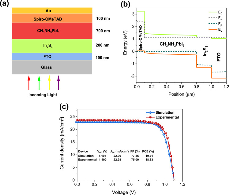
Here, we simulated a typical n-i-p PV architecture with CH3NH3PbI3 perovskite as the photoactive film, compact In2S3 as the ETM, and Spiro-OMeTAD organic film as the HTM, with fluorine-containing SnO2 (FTO) and gold (Au) as the front and back electrodes, respectively. In Fig. 1a, we have a graphical diagram of the FTO/In2S3/CH3NH3PbI3/Spiro-OMeTAD/Au device assembly. Tables 1 and 2 summarize the fundamental device parameters of several materials utilized in this analysis that were acquired from the theoretical and experimental literature. The work functions for the front and back electrodes were 4.4 eV and 5.2 eV, respectively. The SCAPS software calculated the absorption spectrum of each layer based on the optical merits of the materials and the geometry of the device.
Figure 1.
(a) Solar cell structure utilized in simulation. (b) Band alignment diagram of the proposed OPSC. (c) A representation comparison between experimental and modeled parameters of our control OPSC33.
Table 1.
The input parameters of simulated perovskite solar cells.
| Device layer properties | Device layers | ||||
|---|---|---|---|---|---|
| Unit | In2S3 | IGZO | MAPbI3 | Spiro-OMeTAD | |
| Thickness | nm | 200 | 200 | 700 (varied) | 100 |
| Energy gap | eV | 2.45 | 3.05 | 1.57 | 3.2 |
| Electron affinity energy | eV | 3.98 | 4.16 | 3.86 | 2.1 |
| µe | cm2/V s | 400 | 15.0 | 8 | 2 × 10⁴ |
| µh | cm2/V s | 210 | 0.1 | 4 | 2 × 10⁴ |
|
Concentration of the shallow acceptor (NA) |
1/cm3 | 0 | 0.0 | 1 × 10¹⁹ (varied) | 1 × 10²⁰ |
|
Concentration of the shallow donor (ND) |
1/cm3 | 1.47 × 10¹⁸ | 1.0 × 10¹⁸ | 1 × 10¹⁹ | 0 |
| CB effective density of states (NC) | 1/cm3 | 1.8 × 10¹⁹ | 5.8 × 10¹⁸ | 1 × 10¹⁸ | 2.8 × 10¹⁸ |
| VB effective density of states (NV) | 1/cm3 | 4 × 10¹³ | 5.8 × 10¹⁸ | 1 × 10¹⁸ | 1.8 × 10¹⁹ |
| Dielectric permittivity | – | 6.5 | 10.0 | 28 | 3 |
| Defect type | – | Neutral | Neutral | Neutral | Neutral |
| Capture cross section of electrons | cm2 | 1 × 10–15 | 1 × 10–15 | 1 × 10–15 | 1 × 10–15 |
| Capture cross section of holes | cm2 | 1 × 10–15 | 1 × 10–15 | 1 × 10–15 | 1 × 10–15 |
| NT | 1/cm3 | 1 × 10¹⁶ (varied) | 1.0 × 10¹⁵ | 2.45 × 10¹⁵ (varied) | 1 × 10¹⁴ |
| Energetic distribution | – | Single | Single | Single 0.6 eV above Ev | Single 0.6 eV above Ev |
| References | 43 | 44 | 45 | 46 | |
Table 2.
Interface parameters of FTO/ In2S3/MAPbI3/Spiro-OMeTAD/Au OPSCs.
| Parameters/interfaces | In2S3/MAPbI3 | MAPbI3/spiro-OMeTAD |
|---|---|---|
| Defect type | Neutral | Neutral |
| Total defect density (cm−2) | 1 × 10¹⁰ | 1 × 10¹⁰ |
| Capture cross section electrons (cm2) | 1 × 10¹⁰ | 1 × 10⁻¹⁸ |
| Capture cross section holes (cm2) | 1 × 10⁻¹⁹ | 1 × 10⁻¹⁸ |
| Energetic distribution | Single | single |
| Reference for defect energy level Et | Above the highest Ev | Above the highest Ev |
| Energy with respect to reference (eV) | 0.600 | 0.600 |
| Total density (1/cm2) | 1 × 10¹⁰ | 1 × 10¹⁰ |
The defects were used 0.6 eV above the valence band with a particular energy of 0.1 eV, taking into account the Gaussian energy distribution and the capture cross-section of carriers of 10–15 cm2. The radiative recombination coefficient for perovskite was 2.3 × 10⁻⁹ cm3/s, which was taken into consideration. The modeling analysis added imperfections at the HTM/perovskite and perovskite/ETM interfaces about 1010 cm−2. The conventional AM 1.5 G spectrum and a temperature of 300 K were used for the computations.
Figure 1b displays the band structure diagram for the suggested n-i-p OPSC layout. At the conduction band interface of In2S3 and CH3NH3PbI3, a potential barrier of 0.12 eV exists, which is a beneficial barrier for the better transport of electrons from perovskite to ETM, whereas at the junction of the valence band of perovskite and HTM, holes have to contend with a large barrier of 0.13 eV. The J–V plot of the suggested cell architecture was analyzed after the appropriate layer parameters and operational conditions were determined (as covered in this section). Figure 1c displays the calculated J–V graph and its initial output parameters. We attained a power conversion efficiency (PCE) of 19.71%, which is close to the PCE of 18.83% that has been published experimentally33. A slight mismatch between the experimental and computed results is that in the present research, the FTO and Au layers were utilized as front and back electrodes, where the thickness of front and back contacts cannot be changed. In the experimental research, however, they were employed as layers with appropriate thicknesses.
Ethics approval and consent to participate
This article does not contain any studies with human participants or animals performed by the authors. We comply with the ethical standards. We provide our consent to take part.
Results and discussion
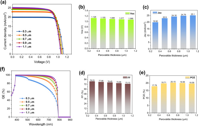
Increasing the device's efficiency is highly dependent on the thickness of the absorber layer. Nevertheless, using a very thick photoactive layer leads to a low charge carrier extraction rate and considerable losses owing to charge recombination; finding the right equilibrium between these two variations is crucial. Therefore, optimizing the light-absorbing thickness becomes essential for determining photocarrier production and spectrum response in photovoltaics47. The obtained J–V graphs are shown in Fig. 2a, with perovskite thickness variations ranging from 0.3 to 1.1 µm, whereas Fig. 2b–e show the variations in the JSC, VOC, FF, and PCE parameters. According to Fig. 2, an increment in the perovskite thickness causes a rise in the JSC and a reduction in the VOC. The trend of rising JSC values is a result of increased photocarrier production. Thin perovskite film results in lower long-wavelength photon absorption rates, which results in less photocarrier formation and worse JSC values48. Furthermore, the poor recombination due to the thin perovskite creates a high VOC. Increasing the absorber perovskite's thickness also boosts the layer's ability to absorb light with longer wavelengths. As a result, more charge carriers are produced, which leads to a rise in the value of the JSC49. However, with higher absorbance, the recombination rate of photocarriers also increases since photocarriers have to cover a longer distance before approaching the corresponding electrodes. The increase in perovskite thickness raises the Rs, which causes a decrease in FF. The improvement in efficiency is attributable to the steady rise in JSC. Our calculations suggest that the ideal value for the perovskite thickness should be 0.7 µm for the highest performance of MAPbI3-based single-cation OPSC. Therefore, optimizing the thickness of the perovskite layer is crucial for achieving the highest efficiency in a perovskite solar cell. By carefully balancing the absorption of light and the extraction of charge carriers, an optimal thickness can be found that maximizes the photocurrent and minimizes recombination, leading to the best performance of the device.
Figure 2.
(a) J–V characteristics of the OPSCs with different MAPbI3 thicknesses. Variations of OPSC performance parameters with various thicknesses of perovskite: (b) VOC, (c) JSC, (d) FF, and (e) PCE. (f) QE of devices with various MAPbI3 thicknesses.
Figure 2f illustrates the external QE (EQE) of devices with varying MAPbI3 film thicknesses. The EQE of the device was clearly improved when the MAPbI3 light harvester thickness was less than 0.7 µm, which indicates that the improvement in absorption was high. Nevertheless, the EQE of the device rose less when the thickness of MAPbI3 was more than 0.7 µm, indicating that the rise in absorption was less significant. As the MAPbI3 film thickness increased, it was better able to absorb light of longer wavelengths50. The profile of carrier generation rate is also obtained and reported in Fig. 3 to validate the higher penetration of generation rate in the absorber layer at higher thicknesses.
Figure 3.
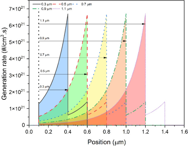
Generation rate inside the device with at different thicknesses of the absorber layer.
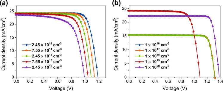
The number of defects in the photoactive MAPbI3 has a significant impact on the output quality of perovskite solar cells. The VOC of the device may be optimized by controlling the generation-recombination rate of the photocarriers inside the perovskite. Shockley–Read–Hall (SRH) recombination may provide a more adequate explanation for the correlation between NT and OPSC performance37,49. The perovskite defect density in this analysis ranges from 2.45 × 10¹⁴ to 2.45 × 1016 cm−3, and its impact on how well our computed work performs is investigated. Figure 4a displays J–V graphs that have been plotted with varying NT values. Results show that a minor decrease in JSC—from 24.241 to 23.582 mA/cm2 and a major reduction in VOC—from 1.188 to 0.991 V—are found when the NT is increased from 2.45 × 10¹⁴ to 2.45 × 1016 cm−3 (Table 3). Since FF is dependent on VOC, there is a significant decrease in FF values (from 79.163 to 66.498%). The efficiency was dramatically reduced from 22.79 to 15.55% because of these decreases in JSC, VOC, and FF values. This suggests that a rise in the NT values leads to a greater number of imperfections, which in turn raises the recombination process, as shown in Fig. 5. According to the experimentally stated value, we chose the NT for the perovskite here to be 2.45 × 1015 cm−3, which accounts for carrier diffusion lengths (Lp) of photocarriers of about 0.65 µm33.
Figure 4.
J–V plots of the OPSCs obtained with varying (a) total defect density and (b) concentration of the shallow acceptor in CH3NH3PbI3.
Table 3.
PV device parameters of OPSCs with varying total defect density in CH3NH3PbI3.
| NT (cm−3) | Lp (µm) | VOC (V) | JSC (mA/cm2) | FF (%) | PCE (%) |
|---|---|---|---|---|---|
| 2.45 × 10¹⁴ | 2.1 | 1.188 | 24.241 | 79.163 | 22.79 |
| 7.55 × 10¹⁴ | 1.2 | 1.138 | 24.227 | 78.347 | 21.60 |
| 2.45 × 10¹⁵ | 0.65 | 1.089 | 24.180 | 76.456 | 20.15 |
| 7.55 × 10¹⁵ | 0.37 | 1.043 | 24.039 | 73.047 | 18.32 |
| 2.45 × 10¹⁶ | 0.21 | 0.991 | 23.582 | 66.498 | 15.55 |
Figure 5.
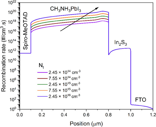
Recombination rate profile at different defect density in absorber layer.
The efficiency of OPSC is significantly affected by the amount of doping used. Doping can be categorized as either n-type or p-type, depending on the dopants used. Thus, improving OPSC efficiency relies on setting the appropriate value of NA. Doping concentration levels can be adjusted experimentally in many different ways51. Doping concentrations and defect density values, for example, can be experimentally modified by adding different dopants or adjusting their concentrations in the perovskite material. Experimentally changing doping ratios and minimizing defects may also be accomplished by adjusting the relative amounts of cesium (Cs), methylammonium iodide (MAI), formamidinium iodide (FAI), and lead iodide (PbI2)52.
Furthermore, the NA of the perovskite was adjusted from 1016 to 1020 cm−3, and the results are shown in Fig. 4b to help understand the impact of doping on the OPSC performance. According to our findings, the J–V characteristics are unchanged at low NA levels. Nevertheless, the inherent built-in electric field (Vbi) rises when NA surpasses 1018 cm−3. The performance of the cell is enhanced by an increase in Vbi because it leads to improved separation of photocarriers. JSC was shown to decrease with increasing NA levels (Table 4). Auger recombination might explain a decline in JSC value with rising NA. Auger recombination rises with increasing doping ratios, which lowers device efficiency53,54. Here, a further decline in JSC was shown if the NA was raised above 1019 cm−3. As a result, we decided to set the highest value for NA in the current simulation at 1019 cm−3.
Table 4.
PV device parameters of OPSCs with varying concentration of the shallow acceptor in CH3NH3PbI3.
| NA (cm−3) | VOC (V) | JSC (mA/cm2) | FF (%) | PCE (%) |
|---|---|---|---|---|
| 1 × 10¹⁶ | 1.319 | 15.382 | 85.548 | 17.36 |
| 1 × 10¹⁷ | 1.319 | 15.382 | 85.523 | 17.35 |
| 1 × 10¹⁸ | 1.316 | 15.381 | 85.236 | 17.26 |
| 1 × 10¹⁹ | 1.090 | 24.180 | 76.469 | 20.16 |
| 1 × 10²⁰ | 1.386 | 22.270 | 86.143 | 26.60 |
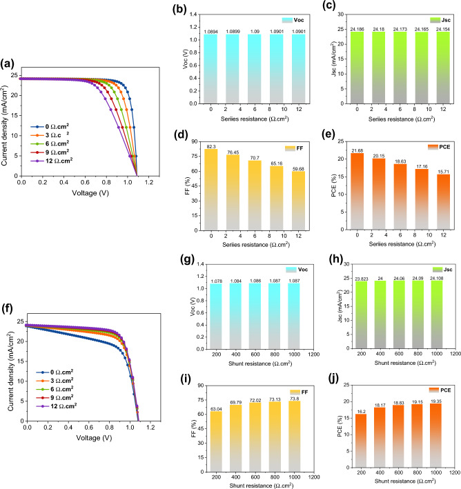
The series resistance (Rs) has a major effect on the operation of the OPSC, particularly the FF and short circuit current (ISC). When the resistance of a series circuit rises, FF drops. Therefore, for higher levels of Rs, the ISC begins to decrease as well. Hence, a device's efficiency suffers when Rs is quite high55. This led researchers to examine how the PCE and FF of perovskite photoactive material changed with variations in Rs. We evaluate the performance of the OPSC while changing the Rs from 0 to 12 Ω cm2 to examine the impact of Rs on OPSC performance. The J–V profiles for various resistances are depicted in Fig. 6a. Our research shows that the photovoltaic has superior performance and a higher FF at lower Rs (Fig. 6b–e). The efficiency of the devices deteriorates rapidly as the Rs rises. These findings are consistent with those reported in other studies36,56.
Figure 6.
(a) J–V characteristics of the OPSCs with different series resistances. Variations of OPSC performance parameters with various series resistances: (b) VOC, (c) JSC, (d) FF, and (e) PCE. (f) J–V characteristics of the OPSCs with different shunt resistances with constant series resistance of 3 Ω cm2. Variations of OPSC performance parameters with various shunt resistances: (g) VOC, (h) JSC, (i) FF, and (j) PCE.
Shunt resistance (Rsh) is caused by the several pathways for charge recombination in the OPSC57. We simulate the device's operation, changing the Rsh from 0 to 1000 Ω cm2, to examine the impact of Rsh on OPSC performance. Changing Rsh affects several different device characteristics, as seen in Fig. 6f,j. The performance of OPSC is found to improve as Rsh rises. PCE = 19.15% and FF = 73.13% at 800 Ω cm2, and at 1000 Ω cm2 we obtain PCE = 19.35% and FF = 73.8%, respectively. Therefore, we determine that an Rsh of 800 Ω cm2 is optimal.
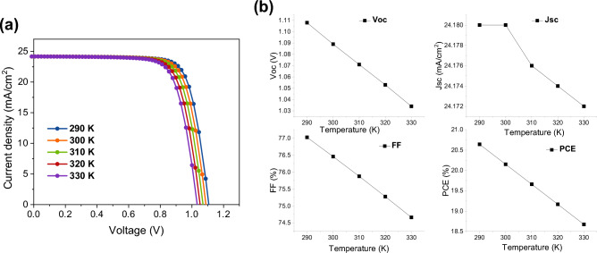
Figure 7a illustrates how altering the ambient temperature from 17 to 57 °C has an impact on the J–V plots of the OPSC device. It turns out that both VOC and FF suffer when the temperature goes up. However, there are not any noticeable changes at JSC. Efficiency gradually drops because both VOC and FF are impacted by rising temperatures. This investigation demonstrates that OPSC in an ambient environment gives better efficiency, which is over 25%; however, as the temperature rises, this efficiency gradually declines, as shown in Fig. 7b. An increase in temperature increases the recombination and reverse saturation currents, which further reduce the VOC and device performance. In addition, when the device is running at a higher temperature, the bandgap gets smaller, which may lead to more exciton recombination and less efficiency58. This observation may be extremely important when choosing OPSC in tropical areas.
Figure 7.
(a) Effect of operational temperature with respect to (a) J–V curves and (b) PV parameters (JSC, VOC, FF, and PCE).
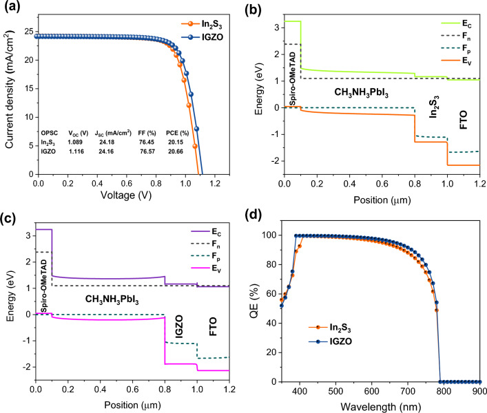
Finally, the performance of the optimized OPSC was compared to that of an OPSC made of indium gallium zinc oxide (IGZO) as an ETM layer (see Fig. 8a). Recently, IGZO has been used as an ETM; it offers great promise because of its high µe, environmental stability, low processing temperatures, and comparable electron affinity to perovskite37,44,59. As we can see in inset table of Fig. 8, In2S3-based device showed comparable photovoltaic parameters to the IGZO-based device. The findings from this study are expected to facilitate the manufacturing of high-efficiency perovskite solar cells in the near future. The energy level layout is constructed by incorporating an ETM, a MAPbI3 absorbing layer, and Spiro-OMeTAD as HTM. This arrangement affects the valence/conduction band offset, which refers to the variation in the valence band between the HTM and the perovskite, as well as the conduction band between the ETM and the perovskite. The energy level offset at the ETM/MAPbI3 and the MAPbI3/HTM interfaces greatly affects the solar cell’s performance36. Figure 8b,c shows that quasi-Fermi levels Fn and Fp coexist with EC and EV in the OPSCs based on In2S3 and IGZO layers. As shown, the In2S3- and IGZO-based structures showed a small conduction band offset (CBO) of 0.121 eV and 0.294 eV at ETM/MAPbI3 interface, indicating that In2S3 ETM provides better interface for electron transportation. However, IGZO film showed larger valence band offset at ETM/MAPbI3 interface, which is significant for blocking the backflow of holes and suppressing the recombination rate in the OPSC.
Figure 8.
(a) J–V curves of perovskite solar cells with different ETMs, including In2S3 and IGZO films. Band offset behaviour of the proposed OPSC based on (b) In2S3 and (c) IGZO. The diagram was calculated using optimized thicknesses of ETMs (200 nm) and MAPbI3 layer (700 nm). (d) EQE of OPSCs with various ETMs at a thickness of 200 nm.
Finally, we estimated The EQE spectra of In2S3 and IGZO ETM-based OPSCs, as shown in Fig. 8d. The EQE could vary depending on the specific features of the semiconductors and the design of the cell. IGZO ETM-based OPSC has been proven to demonstrate relatively higher QE spectrum across the visible spectrum than In2S3 ETM-based OPSC. This is because IGZO has a wide bandgap, which allows it to absorb a minimal amount of visible light while still effectively extracting electrons from the MAPbI3 film. In general, it can be concluded that the utilization of both In2S3 and IGZO ETMs can effectively enhance the EQE of OPSCs. However, the selection of a suitable ETM is dependent upon the specific needs of the device and the preferred wavelength range for optimal performance.
We have provided insights into the relationship between the device's performance and the defects' density, which could be useful for optimizing the fabrication process and improving the device's performance. One possible approach to address this issue is to optimize the growth conditions during the fabrication process to minimize the defect density. For example, by carefully controlling the temperature, pressure, and some other important parameters of spin coating method during the growth process, it is possible to reduce the number of defects in the device. Interface passivation and anion/cation engineering can also be done to reduce the defect density. Additionally, post-growth processing techniques such as annealing could also reduce the density of defects in the material. In summary, we agree that the feasibility of tuning the property of the device at the fabrication or industrial level is an important consideration.
Conclusions
For the first time, the SCAPS-1D model has explored the potential of In2S3 as an alternate ETM film in OPSCs in an effort to increase PV stability, boost efficiency, and reduce hysteresis behavior. Problems with imperfections and high temperatures are fundamental to the simulation analysis. Theoretically, In2S3 can substitute TiO2 as ETL in OPSC, and the results showed that defect states have a significant impact on OPSC efficiency at defect densities higher than 2.45 × 1015 cm−3. Finally, OPSC works best between 20 and 30 °C. The optimized design with an efficiency of 20.15% (VOC = 1.089 V, JSC = 24.18 mA/cm2, and FF = 76.45%) sheds light on the possibility of In2S3 as a suitable ETL. This study paves the way towards practical implementation of indium sulfide as the potential ETL for MAPbI3 perovskite solar cells.
Acknowledgements
The authors extend their appreciation to the University of Warith Al-Anbiyaa (Iraq) for the technical support.
Author contributions
Conceptualization, methodology, software, validation, A.K.A., A.K., S.Q.S., M.K.A.M.; formal analysis, investigation, resources, data curation, writing—original draft preparation, M.K.H., Z.M.Y., D.S.A.; supervision, project administration, D.D., R.P., P.S.J. All authors have read and agreed to the published version of the manuscript. All the authors are giving consent to publish.
Data availability
The datasets used and/or analysed during the current study available from the corresponding author on reasonable request.
Competing interests
The authors declare no competing interests.
Footnotes
Publisher's note
Springer Nature remains neutral with regard to jurisdictional claims in published maps and institutional affiliations.
These authors contributed equally: Mustafa K. A. Mohammed, Ali K. Al-Mousoi and Rahul Pandey.
Contributor Information
Mustafa K. A. Mohammed, Email: mustafa_kareem@yahoo.com
P. S. JosephNg, Email: joseph.ng@newinti.edu.my
References
- 1.Kareem SH, Elewi MH, Naji AM, Ahmed DS, Mohammed MK. Efficient and stable pure α-phase FAPbI3 perovskite solar cells with a dual engineering strategy: Additive and dimensional engineering approaches. Chem. Eng. J. 2022;443:136469. doi: 10.1016/j.cej.2022.136469. [DOI] [Google Scholar]
- 2.Thakur A, Singh D, Gill SK. Numerical simulations of 26.11% efficient planar CH3NH3PbI3 perovskite nip solar cell. Mater. Today Proc. 2022;71:195–201. doi: 10.1016/j.matpr.2022.08.423. [DOI] [Google Scholar]
- 3.Dureja T, Garg A, Bhalla S, Bhutani D, Khanna A. Double lead-free perovskite solar cell for 19.9% conversion efficiency: A SCAPS-1D based simulation study. Mater. Today Proc. 2022;71:239–242. doi: 10.1016/j.matpr.2022.08.518. [DOI] [Google Scholar]
- 4.Abdulzahraa HG, Mohammed MK, Raoof ASM. Electron transport layer engineering with rubidium chloride alkali halide to boost the performance of perovskite absorber layer. Curr. Appl. Phys. 2022;34:50–54. doi: 10.1016/j.cap.2021.11.006. [DOI] [Google Scholar]
- 5.Abdulzahraa HG, Mohammed MK, Raoof ASM. Tin oxide/reduced graphene oxide hybrid as a hole blocking layer for improving 2D/3D hetrostructured perovskite-based photovoltaics. Surf. Interfaces. 2022;31:102092. doi: 10.1016/j.surfin.2022.102092. [DOI] [Google Scholar]
- 6.Li H, et al. Sequential vacuum-evaporated perovskite solar cells with more than 24% efficiency. Sci. Adv. 2022;8:eabo7422. doi: 10.1126/sciadv.abo7422. [DOI] [PMC free article] [PubMed] [Google Scholar]
- 7.Mehde, M. S., Al-Gebori, A. M. & Hantoosh, A. K. In IOP Conference Series: Materials Science and Engineering. 012071 (IOP Publishing).
- 8.Kojima A, Teshima K, Shirai Y, Miyasaka T. Organometal halide perovskites as visible-light sensitizers for photovoltaic cells. J. Am. Chem. Soc. 2009;131:6050–6051. doi: 10.1021/ja809598r. [DOI] [PubMed] [Google Scholar]
- 9.Kim G-H, Kim DS. Development of perovskite solar cells with> 25% conversion efficiency. Joule. 2021;5:1033–1035. doi: 10.1016/j.joule.2021.04.008. [DOI] [Google Scholar]
- 10.Jeong J, et al. Pseudo-halide anion engineering for α-FAPbI3 perovskite solar cells. Nature. 2021;592:381–385. doi: 10.1038/s41586-021-03406-5. [DOI] [PubMed] [Google Scholar]
- 11.Min H, et al. Perovskite solar cells with atomically coherent interlayers on SnO2 electrodes. Nature. 2021;598:444–450. doi: 10.1038/s41586-021-03964-8. [DOI] [PubMed] [Google Scholar]
- 12.Ahmed DS, Mohammed BK, Mohammed MK. Long-term stable and hysteresis-free planar perovskite solar cells using green antisolvent strategy. J. Mater. Sci. 2021;56:15205–15214. doi: 10.1007/s10853-021-06200-w. [DOI] [Google Scholar]
- 13.Jacobsson TJ, et al. An open-access database and analysis tool for perovskite solar cells based on the FAIR data principles. Nat. Energy. 2022;7:107–115. doi: 10.1038/s41560-021-00941-3. [DOI] [Google Scholar]
- 14.Zhao X, et al. Accelerated aging of all-inorganic, interface-stabilized perovskite solar cells. Science. 2022;377:307–310. doi: 10.1126/science.abn5679. [DOI] [PubMed] [Google Scholar]
- 15.Pandey, R. et al. Halide composition engineered a non-toxic perovskite–silicon tandem solar cell with 30.7% conversion efficiency. ACS Appl. Electron. Mater.10.1021/acsaelm.2c01574 (2023).
- 16.Humadi MD, Hussein HT, Mohamed MS, Mohammed MK, Kayahan E. A facile approach to improve the performance and stability of perovskite solar cells via FA/MA precursor temperature controlling in sequential deposition fabrication. Opt. Mater. 2021;112:110794. doi: 10.1016/j.optmat.2020.110794. [DOI] [Google Scholar]
- 17.Kadhim AK, Mohammad MR, Abd Ali AI, Mohammed MK. Reduced graphene oxide/Bi2O3 composite as a desirable candidate to modify the electron transport layer of mesoscopic perovskite solar cells. Energy Fuels. 2021;35:8944–8952. doi: 10.1021/acs.energyfuels.1c00848. [DOI] [Google Scholar]
- 18.Majeed SM, Mohammed MK, Ahmed DS. Efficient and hysteresis-free mixed-dimensional 2D/3D perovskite solar cells using ethyl lactate as a green additive to perovskite precursor solutions. J. Mater. Chem. C. 2022;10:16480–16491. doi: 10.1039/D2TC03313E. [DOI] [Google Scholar]
- 19.Sun H, et al. Interface defects passivation and conductivity improvement in planar perovskite solar cells using Na2S-doped compact TiO2 electron transport layers. ACS Appl. Mater. Interfaces. 2020;12:22853–22861. doi: 10.1021/acsami.0c03180. [DOI] [PubMed] [Google Scholar]
- 20.Hu W, et al. Low-temperature in situ amino functionalization of TiO2 nanoparticles sharpens electron management achieving over 21% efficient planar perovskite solar cells. Adv. Mater. 2019;31:1806095. doi: 10.1002/adma.201806095. [DOI] [PubMed] [Google Scholar]
- 21.You Y, et al. TiO2/WO3 bilayer as electron transport layer for efficient planar perovskite solar cell with efficiency exceeding 20% Adv. Mater. Interfaces. 2020;7:1901406. doi: 10.1002/admi.201901406. [DOI] [Google Scholar]
- 22.Majeed SM, Ahmed DS, Mohammed MK. A novel 3-methylthiophene additive to boost the performance and stability of perovskite solar cells. RSC Adv. 2021;11:10425–10433. doi: 10.1039/D1RA01236C. [DOI] [PMC free article] [PubMed] [Google Scholar]
- 23.Karthick S, Velumani S, Bouclé J. Experimental and SCAPS simulated formamidinium perovskite solar cells: A comparison of device performance. Sol. Energy. 2020;205:349–357. doi: 10.1016/j.solener.2020.05.041. [DOI] [Google Scholar]
- 24.Zhou H, et al. Interface engineering of highly efficient perovskite solar cells. Science. 2014;345:542–546. doi: 10.1126/science.1254050. [DOI] [PubMed] [Google Scholar]
- 25.Singh T, Miyasaka T. Stabilizing the efficiency beyond 20% with a mixed cation perovskite solar cell fabricated in ambient air under controlled humidity. Adv. Energy Mater. 2018;8:1700677. doi: 10.1002/aenm.201700677. [DOI] [Google Scholar]
- 26.Chen P, Yin X, Que M, Liu X, Que W. Low temperature solution processed indium oxide thin films with reliable photoelectrochemical stability for efficient and stable planar perovskite solar cells. J. Mater. Chem. A. 2017;5:9641–9648. doi: 10.1039/C7TA00183E. [DOI] [Google Scholar]
- 27.Kadhim MJ, Mohammed MK. Fabrication of efficient triple-cation perovskite solar cells employing ethyl acetate as an environmental-friendly solvent additive. Mater. Res. Bull. 2023;158:112047. doi: 10.1016/j.materresbull.2022.112047. [DOI] [Google Scholar]
- 28.Widianto E, Rosa ES, Triyana K, Nursam NM, Santoso I. Performance analysis of carbon-based perovskite solar cells by graphene oxide as hole transport layer: Experimental and numerical simulation. Opt. Mater. 2021;121:111584. doi: 10.1016/j.optmat.2021.111584. [DOI] [Google Scholar]
- 29.Wu R, Xu Y, Xu R, Huang Y, Zhang B. Ultrathin-nanosheet-based 3D hierarchical porous In 2 S 3 microspheres: Chemical transformation synthesis, characterization, and enhanced photocatalytic and photoelectrochemical property. J. Mater. Chem. A. 2015;3:1930–1934. doi: 10.1039/C4TA05729E. [DOI] [Google Scholar]
- 30.Hou Y, et al. Low-temperature processed In2S3 electron transport layer for efficient hybrid perovskite solar cells. Nano Energy. 2017;36:102–109. doi: 10.1016/j.nanoen.2017.04.033. [DOI] [Google Scholar]
- 31.Li Y, et al. Hierarchical nanostructures self-assembled from a mixture system containing rod-coil block copolymers and rigid homopolymers. Sci. Rep. 2015;5:1–13. doi: 10.1038/srep10137. [DOI] [PMC free article] [PubMed] [Google Scholar]
- 32.Raj Mohamed J, Sanjeeviraja C, Amalraj L. Effect of substrate temperature on nebulized spray pyrolysised In2S3 thin films. J. Mater. Sci. Mater. Electron. 2016;27:4437–4446. doi: 10.1007/s10854-016-4315-x. [DOI] [Google Scholar]
- 33.Xu Z, Wu J, Yang Y, Lan Z, Lin J. High-efficiency planar hybrid perovskite solar cells using indium sulfide as electron transport layer. ACS Appl. Energy Mater. 2018;1:4050–4056. doi: 10.1021/acsaem.8b00726. [DOI] [Google Scholar]
- 34.Yang B, Wang M, Hu X, Zhou T, Zang Z. Highly efficient semitransparent CsPbIBr 2 perovskite solar cells via low-temperature processed In2S3 as electron-transport-layer. Nano Energy. 2019;57:718–727. doi: 10.1016/j.nanoen.2018.12.097. [DOI] [Google Scholar]
- 35.Burgelman M, Nollet P, Degrave S. Modelling polycrystalline semiconductor solar cells. Thin Solid Films. 2000;361:527–532. doi: 10.1016/S0040-6090(99)00825-1. [DOI] [Google Scholar]
- 36.Al-Mousoi AK, et al. Simulation and analysis of lead-free perovskite solar cells incorporating cerium oxide as electron transporting layer. RSC Adv. 2022;12:32365–32373. doi: 10.1039/D2RA05957F. [DOI] [PMC free article] [PubMed] [Google Scholar]
- 37.Hossain MK, et al. Combined DFT, SCAPS-1D, and wxAMPS frameworks for design optimization of efficient Cs 2 BiAgI 6-based perovskite solar cells with different charge transport layers. RSC Adv. 2022;12:35002–35025. doi: 10.1039/D2RA06734J. [DOI] [PMC free article] [PubMed] [Google Scholar]
- 38.Al-Mousoi AK, et al. Comparative study of the correlation between diffusion length of charge carriers and the performance of CsSnGeI3 perovskite solar cells. Energy Fuels. 2022;36:14403–14410. doi: 10.1021/acs.energyfuels.2c03390. [DOI] [Google Scholar]
- 39.Kumar A, Singh S, Mohammed MK. Numerical investigation of single junction environmental friendly double perovskite (Cs2AuBiCl6) solar cell with 20.5% power conversion efficiency and negligible hysteresis. Int. J. Energy Res. 2022;46:20180–20193. doi: 10.1002/er.8305. [DOI] [Google Scholar]
- 40.Kumar A, Sharma P. Transfer matrix method-based efficiency enhancement of lead-free Cs3Sb2Br 9 perovskite solar cell. Sol. Energy. 2023;259:63–71. doi: 10.1016/j.solener.2023.05.014. [DOI] [Google Scholar]
- 41.Prasanna JL, Goel E, Kumar A. Numerical investigation of MAPbI3 perovskite solar cells for performance limiting parameters. Opt. Quant. Electron. 2023;55:610. doi: 10.1007/s11082-023-04876-9. [DOI] [Google Scholar]
- 42.Burgelman, M., Decock, K., Niemegeers, A., Verschraegen, J. & Degrave, S. SCAPS manual. February (2016).
- 43.Hashemi M, et al. Electrical and optical characterization of sprayed In2S3 thin films as an electron transporting layer in high efficient perovskite solar cells. Sol. Energy. 2021;215:356–366. doi: 10.1016/j.solener.2020.12.046. [DOI] [Google Scholar]
- 44.Rono N, Merad AE, Kibet JK, Martincigh BS, Nyamori VO. Simulation of the photovoltaic performance of a perovskite solar cell based on methylammonium lead iodide. Opt. Quant. Electron. 2022;54:317. doi: 10.1007/s11082-022-03737-1. [DOI] [Google Scholar]
- 45.Chakrabartty J, Islam MA, Reza S. Performance analysis of highly efficient 2D/3D bilayer inverted perovskite solar cells. Sol. Energy. 2021;230:195–207. doi: 10.1016/j.solener.2021.10.007. [DOI] [Google Scholar]
- 46.Elango I, Selvamani M, Ramamurthy PC, Kesavan AV. Studying VOC in lead free inorganic perovskite photovoltaics by tuning energy bandgap and defect density. Ceram. Int. 2022;48:29414–29420. doi: 10.1016/j.ceramint.2022.06.125. [DOI] [Google Scholar]
- 47.Sajid S, et al. Computational study of ternary devices: Stable, low-cost, and efficient planar perovskite solar cells. Nano-micro letters. 2018;10:1–11. doi: 10.1007/s40820-018-0205-5. [DOI] [PMC free article] [PubMed] [Google Scholar]
- 48.Liu D, Gangishetty MK, Kelly TL. Effect of CH 3 NH 3 PbI 3 thickness on device efficiency in planar heterojunction perovskite solar cells. J. Mater. Chem. A. 2014;2:19873–19881. doi: 10.1039/C4TA02637C. [DOI] [Google Scholar]
- 49.Raza E, et al. Numerical simulation analysis towards the effect of charge transport layers electrical properties on cesium based ternary cation perovskite solar cells performance. Sol. Energy. 2021;225:842–850. doi: 10.1016/j.solener.2021.08.008. [DOI] [Google Scholar]
- 50.Zhao P, et al. Numerical simulation of planar heterojunction perovskite solar cells based on SnO2 electron transport layer. ACS Appl. Energy Mater. 2019;2:4504–4512. doi: 10.1021/acsaem.9b00755. [DOI] [Google Scholar]
- 51.Bag A, Radhakrishnan R, Nekovei R, Jeyakumar R. Effect of absorber layer, hole transport layer thicknesses, and its doping density on the performance of perovskite solar cells by device simulation. Sol. Energy. 2020;196:177–182. doi: 10.1016/j.solener.2019.12.014. [DOI] [Google Scholar]
- 52.Tian J, et al. Composition engineering of all-inorganic perovskite film for efficient and operationally stable solar cells. Adv. Funct. Mater. 2020;30:2001764. doi: 10.1002/adfm.202001764. [DOI] [Google Scholar]
- 53.Haider SZ, Anwar H, Wang M. A comprehensive device modelling of perovskite solar cell with inorganic copper iodide as hole transport material. Semicond. Sci. Technol. 2018;33:035001. doi: 10.1088/1361-6641/aaa596. [DOI] [Google Scholar]
- 54.Ghosh A, Dipta SS, Nikor SSS, Saqib N, Saha A. Performance analysis of an efficient and stable perovskite solar cell and a comparative study of incorporating metal oxide transport layers. JOSA B. 2020;37:1966–1973. doi: 10.1364/JOSAB.391817. [DOI] [Google Scholar]
- 55.Heriche H, Rouabah Z, Bouarissa N. New ultra thin CIGS structure solar cells using SCAPS simulation program. Int. J. Hydrogen Energy. 2017;42:9524–9532. doi: 10.1016/j.ijhydene.2017.02.099. [DOI] [Google Scholar]
- 56.Chakraborty K, Choudhury MG, Paul S. Numerical study of Cs2TiX6 (X= Br−, I−, F− and Cl−) based perovskite solar cell using SCAPS-1D device simulation. Sol. Energy. 2019;194:886–892. doi: 10.1016/j.solener.2019.11.005. [DOI] [Google Scholar]
- 57.Pindolia G, Shinde SM, Jha PK. Optimization of an inorganic lead free RbGeI3 based perovskite solar cell by SCAPS-1D simulation. Sol. Energy. 2022;236:802–821. doi: 10.1016/j.solener.2022.03.053. [DOI] [Google Scholar]
- 58.Rono N, Merad AE, Kibet JK, Martincigh BS, Nyamori VO. Optimization of hole transport layer materials for a lead-free perovskite solar cell based on formamidinium tin iodide. Energy Technol. 2021;9:2100859. doi: 10.1002/ente.202100859. [DOI] [Google Scholar]
- 59.Hossain MK, et al. Design and simulation of Cs2BiAgI6 double perovskite solar cells with different electron transport layers for efficiency enhancement. Energy Fuels. 2023;37:3957–3979. doi: 10.1021/acs.energyfuels.3c00181. [DOI] [Google Scholar]
Associated Data
This section collects any data citations, data availability statements, or supplementary materials included in this article.
Data Availability Statement
The datasets used and/or analysed during the current study available from the corresponding author on reasonable request.


