Abstract
The first and foremost intent of our present study is to design a perovskite solar cell favorable for realistic applications with excellent efficiency by utilizing SCAPS-1D. To ensure this motive, the detection of a compatible electron transport layer (ETL) and hole transport layer (HTL) for the suggested mixed perovskite layer entitled FA0.85Cs0.15Pb (I0.85Br0.15)3 (MPL) was carried out, employing diver ETLs such as SnO2, PCBM, TiO2, ZnO, CdS, WO3 and WS2, and HTLs such as Spiro-OMeTAD, P3HT, CuO, Cu2O, CuI, and MoO3. The attained simulated results, especially for FTO/SnO2/FA0.85Cs0.15Pb (I0.85Br0.15)3/Spiro-OMeTAD/Au, have been authenticated by the theoretical and experimental data, which endorse our simulation process. From the detailed numerical analysis, WS2 and MoO3 were chosen as ETL and HTL, respectively, for designing the proposed novel structure of FA0.85Cs0.15Pb (I0.85Br0.15)3-based perovskite solar cells. With the inspection of several parameters such as variation of the thickness of FA0.85Cs0.15Pb (I0.85Br0.15)3, WS2, and MoO3 including different defect densities, the novel proposed structure has been optimized, and a noteworthy efficiency of 23.39% was achieved with the photovoltaic parameters of VOC = 1.07 V, JSC = 21.83 mA cm−2, and FF = 73.41%. The dark J–V analysis unraveled the reasons for the excellent photovoltaic parameters of our optimized structure. Furthermore, the scrutinizing of QE, C–V, Mott–Schottky plot, and the impact of the hysteresis of the optimized structure was executed for further investigation. Our overall investigation disclosed the fact that the proposed novel structure (FTO/WS2/FA0.85Cs0.15Pb (I0.85Br0.15)3/MoO3/Au) can be attested as a supreme structure for perovskite solar cells with greater efficiency as well as admissible for practical purposes.
Nomination of compatible ETL and HTL for the absorber layer FA0.85Cs0.15Pb (I0.85Br0.15)3via numerical analysis.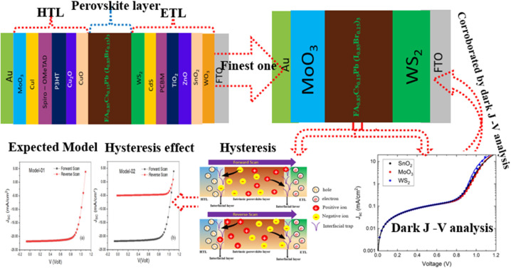
1. Introduction
Perovskites with formula AMX3 (where A, M, and X are organic/inorganic cations, metal cations, and oxygen/halogen anions, respectively) are extremely lucrative materials in the sector of photovoltaic technology owing to their intriguing optoelectronic properties such as tunable band gap, high absorption coefficients, large charge carrier diffusion lengths and high mobility, and ambipolar charge transportation.1,2 Kojima et al.3 first utilized a perovskite material named CH3NH3PbI3 for photovoltaic applications and obtained a power conversion efficiency (PCE) of 3.81%. Perovskite material-based solar cells are gaining substantial attention in terms of efficiency, and throwing challenges to the existing solar cells including silicon-based solar cells. Recently, Min et al.4 reported 25.8% PCE by employing FAPbI3-based solar cells. However, Si-based solar cells are still overshadowing other PSCs due to their high PCE (26.7%5) as well as longevity. In addition to this, a group of scientists from Helmholtz-Zentrum Berlin fabricated tandem solar cells by adopting silicon and perovskite material and attained a world record PCE of 32.5%, which ultimately glorifies the necessity of perovskite material. The composition of the stoichiometric structure of perovskite AMX3 governs the energy band gap, crystal phase, stability as well as performance in photovoltaic applications. The Goldschmidt geometric tolerance factor, 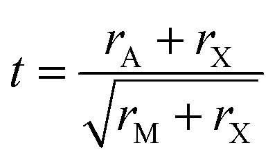 where rA, rM and rX are the effective ionic radii for A, M and X, respectively, determines the formability and stability of a perovskite structure.6 The tolerance factor can be aligned within 0.8–1.0 for steady and worthy structure in photovoltaic technology by partially or fully supplanting the ions of various sites in the AMX3 structure. In a recent study, Liu et al.7 synthesized a perovskite solar cell (PSC) of structure FTO/NiOx/CsPbI3/ZnO/ITO in which the MA cation was substituted by Cs in the perovskite material. They reported a PCE of 16.04%, which was capable to retain 90% PCE even after 3000 hours of constant lighting and heating. In another study, Saliba et al.8 fabricated mixed perovskite structures of Csx(MA0.17FA0.83)1−xPb(I0.83Br0.17)3 and obtained a PCE of 21.1% by utilizing this structure in a PSC. The reported structure was able to hold nearly 97% of its initial efficiency after 250 hours of light exposure.
In another extensive study carried out by Liu et al.9 where they developed a PSC by applying Cs0.05FA0.79MA0.16PbI2.49Br0.51 perovskite structure and claimed that 93% of the initial PCE (21.1%) was maintained under humidity (30–60%) for 1200 hours.
Besides the perovskite material, an efficient PSC has a dependency on ETL, HTL, and the interfacial ETL/perovskite layer and perovskite layer/HTL layers.10 Semiconducting materials are reckoned as charge transport materials that render better transparency in the solar spectrum, broad bandgap, high mobility of charge carriers, and greater thermal and chemical stability. ETL, which extract photo-generated electrons from the perovskite layer and precludes the transfer of hole towards the electrode via ETL, and eventually electron–hole recombination at the interfaces of the perovskite layer gets inhibited. One of the crucial features of selecting ETL is that the energy levels of the material should be compatible with perovskite material to extract electrons and preclude holes. Normally, n-type semiconducting materials such as ZnO, SnO2, CdS, TiO2, WO3, WS2, PCBM, and TMD are broadly esteemed as the ETL. By replacing or modifying the ETL, the overall stability and performance of the PSC can be greatly influenced. Pathak et al.11 modified the ETL of the device Spiro-OMeTAD/CH3NH3PbI3/TiO2 by doping it with Al (0.3 mol%), and subsequently, PCE was increased by approximately 24%. Another analysis was conducted by Song et al.,12 in which, TiO2 was replaced with SnO2 of the architecture Spiro-OMeTAD/CH3NH3PbI3/TiO2 and substantiated 13% PCE. They also emphasized that PSC with SnO2-based solar cells are more stable in comparison with TiO2 based solar cells. In a recent study, Min et al.4 achieved highest PCE (25.8%) by employing SnO2 as an ETL.
HTL provides a pivotal role in extracting photo-generated holes from the perovskite layer and acts as a blocking element for electrons toward the metal electrode. One of the important aspects of choosing HTL is that the energy levels of the material should be relevant to perovskite material for the purpose of hole extraction and blocking the electron. Usually, HTL is a p-type semiconducting material including Spiro-OMeTAD, MoO3, Cu2O, PEDOT:PSS, CuSCN, CuI, PTAA, CuO, and P3HT.
The first ever solid-state HTL (Spiro-OMeTAD) was utilized by Kim20et al. in Kojima's first perovskite, and enhancement of PCE from 3.8% to 9.7% was observed. By substituting or modifying the HTL layer, the overall performance of the PSC can be influenced to some extent. By applying MoO3 instead of PEDOT:PSS and WO3 as the HTL, Tseng et al. synthesize PSCs with the active layer of CH3NH3PbI3 and obtained 13.1% PCE.21 Their analysis distinctively disclosed that in terms of overall performance, the devices manufactured with the MoO3 film are better than the devices employed with WO3 and PEDOT:PSS as the HTL. Since MoO3 has high work function (6.9 eV), better conductivity (1.2 × 10⁻⁷ sm−1) as well as a larger band-gap (>3 eV, no absorption in the visible-infrared range), it has established itself as a competent HTL.22 A schematic diagram of the perovskite structure, n–i–p structured PSC, and equivalent circuit of the PSC are portrayed in Fig. 1.
Fig. 1. A schematic diagram of (a) perovskite structure, (b) n–i–p structure of PSC, and (c) equivalent circuit of the PSC.
In this theoretical work, we have executed a computational analysis by utilizing a solar cell capacitance simulator (SCAPS 1D-3.3.1.0) for choosing compatible ETL and HTL with FA0.85Cs0.15Pb (I0.85Br0.15)3 (MPL) as the mixed perovskite layer. For this motive, primarily, we selected SnO2, PCBM, TiO2, ZnO, CdS, WO3, and WS2 as ETLs. Likewise, Spiro-OMeTAD, P3HT, CuO, Cu2O, CuI, and MoO3 were chosen as HTLs in our proposed n–i–p structure. All initial input physical parameters (IIPPs) of ETL, HTL, and MPL utilized in this simulated study were collected from the previously reported experimental and simulated data. Our prime focus for this research was to identify the structure that serves the best performance. Herein, 42 structures have been formulated by using the aforementioned ETLs and HTLs with MPL, and eventually, the preferred one was found as well. Finally, we have probed the effect of changing thickness, the defect density of MPL, and interfacial defects on our best structure (FTO/WS2/MPL/MoO3/Au). In addition, the impact of ETL's shallow uniform donor density on the C–V and M–S plots of the optimized structure was scrutinized. Moreover, QE analysis and the hysteresis effect of the optimized structure were dissected. Finally, the dark J–V analysis was executed to unravel the reasons behind the tremendous photovoltaic parameters of our optimized structure. To the best of our knowledge, this is the first-ever comprehensive study on this unique structure.
2. Computational details
SCAPS, developed by the University of Gent, is a one-dimensional and proficient solar cell simulator among other simulators (SILVACO, ATLAS, AMPS, COMSOL, etc)23–25 and it is widely used to realize the essence of energy band structure, I–V characteristics, C–V analysis, M−S analysis, doping profile, C-f study, spectral response, etc., of a solar cell. SCAPS-1D is governed by three fundamental eqn (i)–(iii) named continuity equations for holes and electrons, and Poisson's equations to fortuitously complete its task under equilibrium conditions.
 |
i |
 |
ii |
 |
iii |
where ξ represents the electric field, ε represents permittivity, q is the electronic charge, τ is the carrier lifetime, charge mobilities are indicated by μ, shallow acceptor and shallow donor concentrations are represented NA and ND, respectively, D represents the diffusion coefficient of the charge carrier, the charge carrier generation rate is indicated by G, and defect densities of electrons and holes are mentioned by nt(x) and pt(x).
3. Results and discussions
In a previous study, Karthick et al.13 synthesized FTO/SnO2/FA0.85Cs0.15Pb(I0.85Br0.15)3/Spiro-OMeTAD/Au-based PSC structure and obtained VOC = 1 V, Jsc = 22.6 mA cm−2, FF = 64.4% and PCE = 15.1%. We simulated this structure by using SCAPS to corroborate and compare it with the experimental results. In this simulation, we considered the realistic facts by inserting bulk defects, amphoteric defects, interfacial defects, resistance, etc., and the rest of the IIPPs of the different layers were rendered from different published studies, as shown in Table 1. We maintained the following data in all defect layers for all simulations: the defect type was neutral, energetic distribution was Gaussian, characteristic energy was 0.1 eV, and energy level with respect to reference 0.6 eV and electron/hole capture cross-section 10−15 cm2. We also added interfacial defects at the MPL/ETL and MPL/HTL layers with 2 × 1011 cm−3 and 2 × 1010 cm−3, respectively, in which the electron/hole capture cross section was 10−19 cm2. In addition to that, amphoteric defect of 2 × 1015 cm−3 was included in the proposed MPL. Furthermore, we performed the simulation by considering constant light illumination of 1000 Watt per m2 at 1.5 AM ranging from 300–1000 at a temperature of 300 K, series resistance of 3 Ω cm2, and shunt resistance of 5000 Ω cm2.
IIPPs for each layer of the PSC collected from ref. 13.
| Parameters | FTO | SnO2 | FA0.85Cs0.15Pb (I0.85Br0.15)3 | Spiro-OMeTAD | Au |
|---|---|---|---|---|---|
| Thickness (t) in nm | 500 | 70 | 350 | 165 | — |
| Band gap (Eg) in eV | 3.5 | 3.5 | 1.59 | 2.9 | — |
| Electron affinity (χ) in eV | 4 | 4 | 4.09 | 2.2 | — |
| Dielectric permittivity (εr) | 9 | 9 | 6.6 | 3 | — |
| CB effective density of states (Nc) in cm−3 | 2.2 × 10¹⁸ | 2.2 × 10¹⁷ | 2 × 10¹⁹ | 2.2 × 10¹⁸ | — |
| VB effective density of states (Nv) in cm−3 | 2.2 × 10¹⁸ | 2.2 × 10¹⁷ | 2 × 10¹⁸ | 2.2 × 10¹⁸ | — |
| Electron thermal velocity (Ve) in cm s−1 | 1 × 10⁷ | 1 × 10⁷ | 1 × 10⁷ | 1 × 10⁷ | — |
| Hole thermal velocity (Vh) in cm s−1 | 1 × 10⁷ | 1 × 10⁷ | 1 × 10⁷ | 1 × 10⁷ | — |
| Electron mobility (μe) in cm2 V−1 s−1 | 20 | 20 | 8.16 | 0.0001 | — |
| Hole mobility (μh) in cm2 V−1 s−1 | 10 | 10 | 2 | 0.0001 | — |
| Shallow uniform acceptor density (NA) in cm−3 | 0 | 0 | 1.3 × 10¹⁶ | 1.3 × 10¹⁸ | — |
| Shallow uniform donor density (ND) in cm−3 | 1 × 10¹⁵ | 1 × 10¹⁵ | 1.3 × 10¹⁶ | 0 | — |
| Defect density (Nt) in cm−3 | 1 × 10¹⁸ | 1 × 10¹⁸ | 4 × 10¹³ | 1 × 10¹⁵ | — |
| Amphoteric defect density (ADD) in cm−3 | — | — | 2 × 10¹⁵ | — | — |
| Work function (φ) in (eV) | — | — | — | — | 5.3 |
The obtained photovoltaic parameters (PPs) of the structured PSC (S1) were as follows VOC = 0.96 V, JSC = 20.03 mA cm−2, FF = 53.84% and PCE = 14.12%. This simulated result is consistent with the aforementioned experimental results, which vindicated the validity of our simulation.
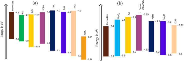
To observe the finest structures with performance, 42 structures were constructed and simulated by varying different ETLs and HTLs with the aforementioned proposed MPL. The IIPPs of ETLs and HTLs are tabulated in Tables 1 and 2. The simulated results of the 42 structures are displayed in Tables 3 and TSI 01.† Different values of PPs were demonstrated by dissimilar structures depending on the band alignment (as shown in Fig. 2) of ETLs and HTLs with MPL. The CBO between MPL and ETLs, and VBO between MPL and HTLs indicate the condition of band alignment. For positive/negative values of VBO and CBO, a spike/cliff is established.35 In the case of negative VBO, there is no hindrance of flowing holes to the back electrode. However, the increment of negative VBO gives rise to interfacial recombination. On the other hand, for negative CBO, the electron can simply drift to ETL.36 However, for positive CBO (0–0.3 eV), low interfacial recombination and selective charge collection occurred.14 The CBO and VBO calculated by using the following eqn (iv) and (v) are displayed in Table 4.
| CBO = χMPL − χETL | iv |
| VBO = (χHTL + EgHTL) − (χMPL + EgMPL) | v |
where, χMPL/χETL/χHTL is the electron affinity of MPL/ETL/HTL, respectively, and EgMPL/EgHTL is band gap of MPL/HTL, respectively. Although CBO between MPL and WO3 possesses the highest value than that for CBO between MPL and WS2, better performance was exhibited by the structure with WS2 as ETL. With the large band gap as well as the existence of valence band maxima in relatively lower energy as compared to WS2, it may create inhibition in hole transportation. As a result, it offers lower performance compared to the structure with WS2.
IIPPs of ETLs and HTLs.
| ETLs | HTLS | ||||||||||
|---|---|---|---|---|---|---|---|---|---|---|---|
| Parameters | PCBM | TiO2 | ZnO | CdS | WO3 | WS2 | P3HT | CuO | Cu2O | CuI | MoO3 |
| t (nm) | 70 | 70 | 70 | 70 | 70 | 70 | 165 | 165 | 165 | 165 | 165 |
| E g (eV) | 2 | 3.2 | 3.3 | 2.4 | 2.6 | 1.8 | 2 | 1.48 | 2.17 | 3.1 | 3 |
| χ (eV) | 4.2 | 4.1 | 4.1 | 4.18 | 3.8 | 3.95 | 3.2 | 4.07 | 3.2 | 2.1 | 2.5 |
| ε r | 3.9 | 9 | 9 | 10 | 4.8 | 13.6 | 3 | 18.1 | 7.11 | 6.5 | 12.5 |
| N c (cm−3) | 2.5 × 10²¹ | 2.2 × 10¹⁸ | 2.2 × 10¹⁸ | 2.2 × 10¹⁸ | 2.2 × 10²¹ | 2.2 × 10¹⁷ | 1 × 10²⁰ | 2.1 × 10¹⁹ | 2 × 10¹⁷ | 2.8 × 10¹⁹ | 2.2 × 10¹⁸ |
| N v (cm−3) | 2.5 × 10²¹ | 1 × 10¹⁹ | 1.9 × 10¹⁹ | 1.9 × 10¹⁹ | 2.2 × 10²¹ | 2.2 × 10¹⁶ | 1 × 10²⁰ | 5.5 × 10¹⁹ | 1.1 × 10¹⁹ | 1 × 10¹⁹ | 1.8 × 10¹⁹ |
| V e (cm s−1) | 1 × 10⁷ | 1 × 10⁷ | 1 × 10⁷ | 1 × 10⁷ | 1 × 10⁷ | 1 × 10⁷ | 1 × 10⁷ | 1 × 10⁷ | 1 × 10⁷ | 1 × 10⁷ | 1 × 10⁷ |
| V h (cm s−1) | 1 × 10⁷ | 1 × 10⁷ | 1 × 10⁷ | 1 × 10⁷ | 1 × 10⁷ | 1 × 10⁷ | 1 × 10⁷ | 1 × 10⁷ | 1 × 10⁷ | 1 × 10⁷ | 1 × 10⁷ |
| μ e (cm2 V−1 s−1) | 0.2 | 20 | 100 | 100 | 30 | 100 | 1 × 10⁻⁴ | 100 | 200 | 100 | 25 |
| μ h (cm2 V−1 s−1) | 0.2 | 10 | 25 | 25 | 30 | 100 | 1 × 10⁻⁴ | 0.1 | 80 | 43.9 | 100 |
| N A (cm−3) | 0 | 0 | 0 | 0 | 0 | 0 | 1 × 10¹⁶ | 1 × 10¹⁶ | 1 × 10¹⁸ | 1 × 10¹⁸ | 1 × 10¹⁸ |
| N D (cm−3) | 2.93 × 10¹⁷ | 1 × 10¹⁸ | 1 × 10¹⁸ | 1 × 10¹⁸ | 6.35 × 10¹⁷ | 1 × 10¹⁸ | 0 | 0 | 0 | 0 | 0 |
| N t (cm−3) | 1 × 10¹⁴ | 1 × 10¹⁴ | 1 × 10¹⁵ | 1 × 10¹⁵ | 1 × 10¹⁵ | 1 × 10¹⁵ | 1 × 10¹⁵ | 1 × 10¹⁴ | 1 × 10¹⁵ | 1 × 10¹⁵ | 1 × 10¹⁵ |
| Ref. | 15 | 26 and 27 | 26 | 28 | 29 | 30 | 27 and 31 | 15 | 32 | 33 | 34 |
Performance of various PSC structures.
| Name of the structure | V oc (V) | J sc (mA cm−2) | FF (%) | η (%) |
|---|---|---|---|---|
| FTO/SnO2/MPL/Spiro-OMeTAD/Au (S1) | 0.96 | 20.09 | 53.84 | 14.12 |
| FTO/SnO2/MPL/Cu2O/Au (S4) | 1.09 | 20.42 | 64.60 | 19.64 |
| FTO/SnO2/MPL/MoO3/Au (S6) | 1.08 | 20.19 | 68.84 | 20.40 |
| FTO/TiO2/MPL/Cu2O/Au (S16) | 1.11 | 20.47 | 70.58 | 21.77 |
| FTO/TiO2/MPL/MoO3/Au (S18) | 1.09 | 20.22 | 75.13 | 22.58 |
| FTO/ZnO/MPL/Cu2O/Au (S22) | 1.11 | 20.47 | 70.58 | 21.77 |
| FTO/ZnO/MPL/MoO3/Au (S24) | 1.09 | 20.22 | 75.13 | 22.58 |
| FTO/CdS MPL/Cu2O/Au (S28) | 1.11 | 20.51 | 70.31 | 21.70 |
| FTO/CdS/MPL/MoO3/Au (S30) | 1.09 | 20.30 | 75.03 | 22.60 |
| FTO/WO3/MPL/Cu2O/Au (S34) | 1.11 | 20.48 | 70.59 | 21.79 |
| FTO/WO3/MPL/MoO3/Au (S36) | 1.09 | 20.25 | 75.12 | 22.61 |
| FTO/WS2/MPL/Cu2O/Au (S40) | 1.11 | 20.87 | 70.41 | 22.16 |
| FTO/WS2/MPL/MoO3/Au (S42) | 1.09 | 20.71 | 74.93 | 23.10 |
Fig. 2. Relative alignment of the energy band of FA0.85Cs0.15Pb (I0.85Br0.15)3 (MPL) with (a) ETLs and (b) HTLs.13–19.
CBO and VBO of the MPL with ETLs and HTLs.
| ETL | PCBM | TiO2 | SnO2 | ZnO | CdS | WO3 | WS2 | HTL | Spiro-OMeTAD | P3HT | CuO | Cu2O | CuI | MoO3 |
|---|---|---|---|---|---|---|---|---|---|---|---|---|---|---|
| CBO | −0.11 | −0.01 | 0.09 | −0.01 | −0.09 | 0.29 | 0.14 | VBO | −0.75 | −0.48 | −0.13 | −0.31 | −0.48 | −0.18 |
From Tables 3 and TSI 01,† we have distinguished S4, S6, S16, S18, S22, S24, S28, S30, S34, S36, S40, and S42 as aspiring structures from 42 formulated structures according to their performance. S42 structure was the most satisfactory one among all the simulated devices, in which WS2 and MoO3 were utilized as ETL and HTL, respectively, and the obtained PPs were VOC = 1.09 V, JSC = 20.71 mA cm−2, FF = 74.93%, and PCE = 23.10%. For further investigation of our research work, we extensively focused on optimizing the structure S42 by varying the different parameters of the layers.
3.1. Thickness optimization
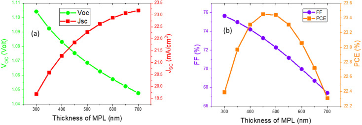
The effect of changing MPL thickness was carried out from 300 nm to 700 nm while thicknesses of both ETL and HTL were sustained at 50 nm. The photovoltaic parameter JSC was increased by 17.81% from the initial value. However, FF and VOC were dropped 10.88% and 5.1%, respectively, from their original value owing to the change in MPL thickness. The decline meant that VOC is happened due to the decrease in dark saturation current with the increase in thickness of the MPL.37 In the case of FF, it showed declining behavior due to the increase in series resistance with the rise in the MPL thickness.38 The positive gradient of current density at lower thickness is comparatively higher up to 450 nm after that the rate slowed down gradually. With increasing thickness, the absorption of a photon is more and consequently generates more electron–hole pairs. As a result, JSC was eventually increased. After 450 nm thickness, rate of increasing JSC becomes slow because of the dominating recombination rate.
Another important photovoltaic parameter, PCE increases with the increase in thickness of the MPL up to 450 nm at which maximum PCE was observed (23.45%) and then a slumping pattern was noticed till 700 nm. With the increasing thickness after 450 nm, PCE decreases due to the increase in series resistance and the recombination rate may also get higher owing to the lower diffusion length compared to the thickness.39 The thickness of the MPL was optimized at 450 nm due to the aforementioned reason and the PPs were 1.08 V, 21.84 mA cm−2, 73.28%, and 23.45% for VOC, JSC, FF and PCE, respectively. Variations of PPs with respect to MPL thickness are displayed in Fig. 3.
Fig. 3. Variation of the device characteristics, such as VOC, JSC, FF, and PCE with respect to the thickness of the MPL.
The precise selection of parameters for ETL and HTL is crucial for fabricating highly efficient solar cells. The careful selection of ETL helps to minimize the recombination current and significantly enhances the transmittance, leading to improved overall performance.40 To optimize the thickness of ETL, the thickness was changed from 10 nm to 100 nm and the thicknesses of the MPL and HTL were kept constant at 350 nm and 70 nm, respectively. The PCE of the device increased by 2.7% from the initial PCE of 22.66% and the change of other PPs was not a significant amount, which is displayed in Fig. FSI 1.† By considering the feasibility of the fabrication technique, we fixed the optimization value of ETL thickness at 50 nm. At 50 nm, the PPs for VOC, JSC, FF and PCE were 1.0924 V, 20.58317 mA cm−2, 74.99%, and 22.97% respectively. Similarly, the thickness of the HTL was also varied from 10–100 nm by holding MPL thickness at 350 nm and ETL thickness at 50 nm. Owing to this, the change in PCE was noted slightly up to 50 nm, however, after 50 nm, the value was constant, which is displayed in Fig. FSI 2.† By analyzing the simulated data, the HTL thickness was optimized at 50 nm. From the clear inspection of our results, it is evident that the thickness of ETL and HTL imposes a very slight influence on the performance, which is also justified through previous works.40,41
3.2. Defects optimization
Defect density can be termed as a dominant parameter that deleteriously influences the performance of the device. The amount of charge carriers that can reach the respective electrode, which is initiated from the perovskite layer, greatly relies on this defect density. The recombination process is expedited with the increasing defect density at the perovskite layer. The relation between the recombination process to the defect density of the perovskite layer is illustrated by the Shockley–Read–Hall (SRH)42 recombination model (vi) as follows;
 |
vi |
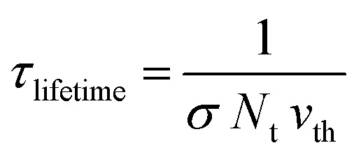
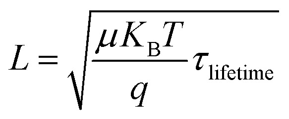
where, υth is the thermal velocity of charge carriers, σn/σp is the capture cross-section of electrons/holes, Nt is the number of defects per unit volume, n/p is the equilibrium electron/hole concentration, ni is the intrinsic carrier concentration and n1/p1 is the concentration of electron/holes at trap states/valence band, respectively. The impact of the defect density on the lifetime of the carrier and diffusion length is explicated by the following eqn (vii) and (viii),43
 |
vii |
 |
viii |
where, τlifetime is the lifetime of the charge carrier, L is the charge carrier diffusion length and μ is the mobility of the charge carrier.
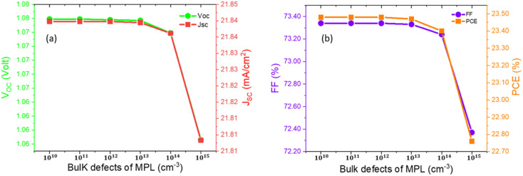
To examine the impact of bulk defect density of MPL, the defect density was varied from 1010 cm−3 to 1015 cm−3. All the PPs showed insignificant change with the bulk defect density and the PPs such as VOC, JSC, FF and PCE were changed by 1.6%, 0.17%, 1.32%, and 3.07%, respectively. The PPs were almost constant up to 1014 cm−3 bulk defect density. Hence 1014 cm−3 is termed as the tolerable bulk defect density of the structure. After that, the PPs decreased gradually with the increase in the defect density owing to the decrease in diffusion length, which results in increased bulk recombination as explained in the above equation. Variations of PPs owing to changing bulk defect density are shown in Fig. 4. Improving the crystalline quality and having a larger grain size have been proven to be advantageous to lessen the effect of the bulk defect. To perform this, photo-curing and thin-film post-processing can be employed.44
Fig. 4. Variation of the device characteristics, such as VOC, JSC, FF, and PCE with respect to bulk defects of the MPL.
Interfacial trap density critically influences the PPs. In a perovskite material having a large absorption coefficient, photo-generated charge carrier numbers are high at the light illumination side compared to the backside. Interface recombination center has a greater impact on the probability of charge collection than severe recombination centers.
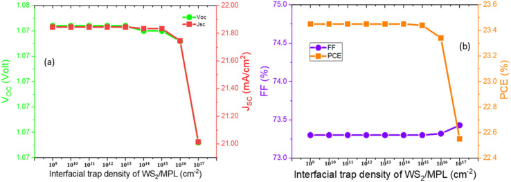
If light enters the perovskite structure through ETL, then the recombination rate at the ETL/perovskite layer interfaces is greater compared to the perovskite layer/HTL interfaces due to the generation of more electron–hole pairs. Poor interface quality severely influences the performance of the PSC. As a consequence of generating more electron–hole pairs in the ETL/perovskite layer interface because of light traveling from ETL to HTL via the absorbing layer, the rate of recombination was found higher in the ETL/perovskite layer interface than in the HTL/perovskite layer. For this reason, the ETL/perovskite interfacial layer is more sensitive. To analyze the effect of interfacial defects on the PPs, the interfacial trap density at WS2/FA0.85Cs0.15Pb (I0.85Br0.15)3 was varied from 1010 cm−3 to 1017 cm−3. No appreciable change was noticed for the PPs up to 1015 cm−3. After 1015 cm−3, PCE starts to decrease gradually. Changes in PPs concerning the interfacial traps of WS2/MPL are depicted in Fig. 5.
Fig. 5. Variation of the device characteristics, such as VOC, JSC, FF, and PCE with respect to the interfacial trap density of WS2/MPL.
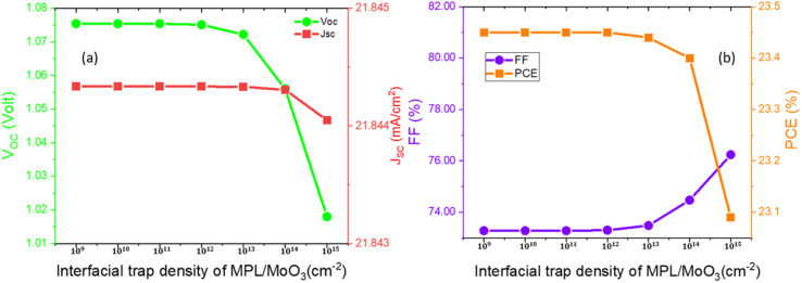
The interfacial trap density at FA0.85Cs0.15Pb (I0.85Br0.15)3/MoO3 was altered as well from 1010 cm−3 to 1015 cm−3 to visualize the impact on PPs. Variations of PPs for interfacial defects of MPL/MoO3 are depicted in Fig. 6. The PPs remain unchanged up to 1013 cm−3 and after that, the PPs show a slight reduction. Because of the variation of interfacial defect density at ETL/MPL as well as MPL/HTL, reductions by 3.5% and 1.5% in PCE were detected, respectively. A greater recombination rate is the sole reason for the reduction in PPs with the increase in interfacial defect density. By weighing the above facts, 1015 cm−3, and 1013 cm−3 were reckoned as the optimized interfacial trap density at ETL/MPL and MPL/HTL layers, respectively. To improve the band alignment between ETL/MPL and MPL/HTL layers, as well as to eradicate the defects and trap states in the interfacial layer, a buffer layer or additives with ETL or HTL can be a beneficial solution.45,46 However, in both cases, the FF is slightly increased at the higher trap densities. To know the essence of this behavior of the FF parameter, further investigation is required.
Fig. 6. Variation of the device characteristics, such as VOC, JSC, FF, and PCE with respect to the interfacial trap density of MPL/MoO3.
3.3. Impact of defect density and thickness on quantum efficiency
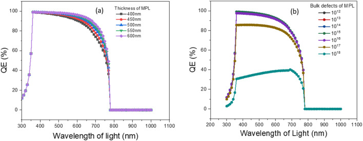
The efficiency of the photovoltaic device can be calculated from IQE and EQE, where IQE refers to the total photocurrent generated under light illumination and EQE implies the optical performance of the PSC.47–49 To realize the consequences of differing thickness on quantum efficiency, the MPL thickness was changed and the results are illustrated in Fig. 7a. For a thickness of 300 nm, the maximum quantum efficiency was 97.54% at a wavelength of 360 nm. Thickness range from 400 nm to 600 nm, the maximum quantum efficiency of about 99% was detected at 360 nm. An unnoticeable change of absorption has been observed after the 780 nm wavelength of light. All of our modeled structures showcased a noteworthy amount of QE, for the range of visible light. Our proposed structure having a thickness of 450 nm, 98.8%, and 77.9% QE was assessed at wavelengths of 400 nm and 700 nm, respectively. Greater QE implied a larger collection of charge carriers, which signifies that our simulated structure demonstrated the best performance under visible light. The inspection was executed carefully to realize the outcome of altering the bulk density of MPL on QE by varying the bulk density from 1012 cm−3 to 1018 cm−3 and the obtained results are depicted in Fig. 7b. Approximately, 98.5% QE was encountered for defect density of up to 1016 cm−3 at a wavelength of 360 nm of light. However, the severe slump in QE was found after 1016 cm−3 and detection of 40% QE at 1018 cm−3 defect density in which the light wavelength was 690 nm. Unnoticeable absorption was observed after the 780 nm wavelength of light for all defect densities. In our proposed structure, having defect density of 1014 cm−3, QE values were 99% to 78% at around 400 nm and 700 nm wavelength, respectively. Thus, this structure exhibits the best spectral response under visible light.
Fig. 7. Variation of QE owing to (a) thickness and (b) bulk defects of MPL.
3.4. Capacitance–voltage characteristics of the PSC
The capacitance–voltage (C–V) technique can also be regarded as another salient technique for characterizing a solar cell by employing SCAPS-1D. Our present study emphasized exploring the outcome of ETL's ND on C–V as well as the Mott–Schottky plot (M−S). Built-in potential, a foremost parameter, which is necessary for accumulating photo-generated holes and electrons in opposite directions from each other, can be acquired from the M−S plot. The capacitance of a PSC can be correlated with the built-in potential by the following formula (ix),50
 |
ix |
where V = applied voltage, Vbi = built-in potential, A = area, C = Capacitance, NA= dopant density, and ε = permittivity of the vacuum medium.
Because of the influence of space charge, a larger capacitance value can be attained, which ultimately lowers the value of built-in potential. The recombination rate in a solar cell is notably lowered with the larger built-in potential, therefore, the attainment of greater PCE may be possible. After a definite range of voltage, the slope of capacitance can be negative. This negative capacitance may also be created from recombination or self-heating.
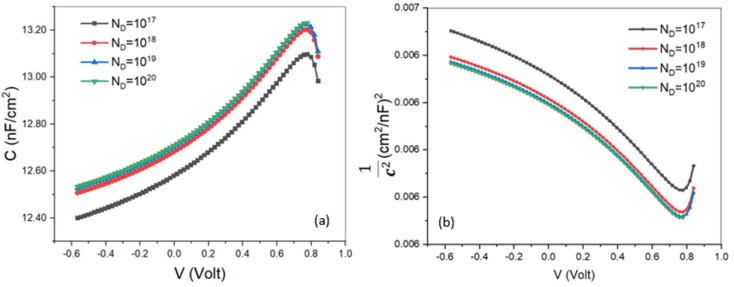
To probe the consequences of ETL's ND on the C–V and Mott–Schottky plots, this density was changed from 1017 cm−3 to 1020 cm−3 and the obtained results are mapped in Fig. 8. An identical graphical pattern for capacitance against voltage was found for all the varied donor densities, where, capacitance revealed exponentially increasing behavior with voltage until the approximate value of the voltage 0.78 V. This phenomenon can be narrated as a large number of electrons being confined in the space charge region (SCR). In other words, a trivial amount of recombination of electron–hole pairs has happened in that region. After this certain value (0.78 V), capacitance manifested a sudden drop, offering a negative slope. The reason behind this can be ascribed in terms of the transformation of electron traps into hole traps in the SCR. According to the inspection of Burgelman et al.51 on defect density, the lowering rate of electron density traps is equivalent to the growth rate of hole density traps in the SCR, which implies the alteration of electron traps into hole traps. The maximum capacitances were assessed as 13.23 nF cm−2, 13.22 nF cm−2, 13.20 nF cm−2, and 13.09 nF cm−2 for uniform shallow donor densities of 1020 cm−3, 1019 cm−3, 1018 cm−3, and 1017 cm−3, respectively. From the scrutiny of the Mott–Schottky plot, the built-in potential was attained as 1.0 V to 0.85 V from the approximate intersection point at the horizontal axis for every graph with the ND of 1017 cm−3 to 1020 cm−3. Photo-generated holes and electrons can efficaciously proceed towards the respective electrode under the dominance of a larger built-in potential that finally provides us with higher conversion efficiency. In accordance with our inspection, the rising of donor density lowers the value of built-in potential owing to the elevation of the trapped electron in SCR that ultimately gives an increment in capacitance.
Fig. 8. (a) C–V characteristics and (b) MS plot as a function of ETL's ND.
3.5. Hysteresis effect on the performance of the PSC
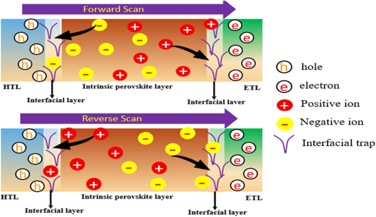
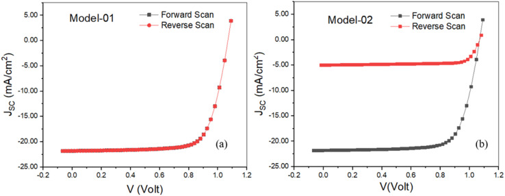
Ion migration and ion accumulation at the interfaces (portrayed in Fig. 9) under biasing voltage are one of the aspects involved in creating hysteresis in the J–V characteristics of a PSC.52 Two types of models entitled Model-01 where ETL and HTL defects were termed as donor type and acceptor type defects, respectively, keeping the other defects as neutral type. In Model-02, defects of HTL/MPL, as well as MPL/ETL, were considered acceptor-type defects and donor-type defects, respectively, whereas MPL and FTO defects were considered neutral-type defects. In both cases, forward and reverse scans were examined by switching the defect type to investigate hysteresis behavior in the J–V curve. No hysteresis has been noticed in model-1, as shown in Fig. 10a. However, in model-2, the severe impact of hysteresis on the J–V curve was noted, as shown in Fig. 10b. Because of the influence of hysteresis, the amount of JSC and PCE dropped to 76.94% and 75.40%, respectively, whereas VOC showed a steady value in both cases and a slight increment in FF (6.7%) was pointed out as well.
Fig. 9. A schematic of the charge migration and re-orientation in the perovskite layer under the influence of forward and reverse scans.
Fig. 10. Hysteresis effect on the J–V characteristics.
As the interfacial layer is adjacent to the perovskite layer, ion accumulation and/or migration certainly have a significant influence on carrier transportation from perovskite to ETL and HTL. This could be the reason for generating the hysteresis effect in model 2. It has been reported that the J–V hysteresis in PSCs is caused by the localization of positively charged ions at the interface between the ETL and the perovskite layer.53 Furthermore, the localized ions may accelerate non-radiative recombination, resulting in the rapid deterioration of PSCs.53–55 Thus, to assure a reliable structure with the best performance, the proposed model-1 could be the best option.
3.6. Dark current analysis
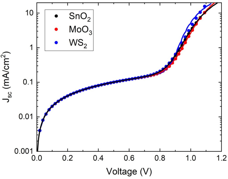
The analysis of dark J–V for a photovoltaic device is an indispensable tool to realize the electrical characteristics in favor of the photovoltaic application. In the p–n junction, as a foundational cause of electronic noise, the dark current has been weighed.56 As a consequence, the performance of the device was interjected. In the p–n junction, the dark current is indicated as the sum of the components of bulk and surface current.57 The tunneling current, diffusion current, and generation–recombination current are part of the bulk component. The leakage shunt current and generation–recombination current are the components of the surface current, which in general appear at the interface of the semiconductor and dielectric devices.57 The essence of the electrical properties of the PSC device can be deciphered by fitting dark J–V characteristics into a single p–n junction model. Fig. 11 shows the dark J–V curves of the optimized perovskite solar cell. The saturated current (I0), series resistance (Rs), shunt resistance (Rsh) and ideality factor (n) are approximated by fitting the following equation onto the J–V characteristics of the proposed device. where k, q, and T are Boltzmann's constant, electronic charge, and temperature, respectively. The dark J–V curve has been plotted by utilizing the simulated data in which the data of current density are applied in logarithmic form (as shown in Figure). The diode characteristics, such as I0, Rs, Rsh, and n of the three different solar cells were extrapolated, as shown in Table 5 by curve fitting using Origin 2018. It can be seen that the lowest saturated current density (I0) of 1.09 × 10⁻¹⁴ mA cm−2 was found for the WS2; this lower value signifies that recombination (defect density) in the depletion region is quite insignificant58 in this structure.
Fig. 11. Dark J–V characteristics of the perovskite solar cells used in model 1.
Diode characteristics of three different ETL with perovskite structure FTO/ETL/FA0.85Cs0.15Pb(I0.85Br0.15)3/MoO3/Au.
| ETL | Saturation current density, I0 (mA cm−2) | Ideality factor, n | Shunt resistance, Rsh (Ω cm2) | Series resistance, Rs (Ω cm2) |
|---|---|---|---|---|
| SnO2 | 4.08 × 10⁻¹³ | 1.38 | 4.96 | 0.00861 |
| MoO3 | 7.31 × 10⁻¹³ | 1.36 | 4.99 | 0.00881 |
| WS2 | 1.09 × 10⁻¹⁴ | 1.10 | 4.78 | 0.00797 |
Moreover, the lowest series resistance 0.00797 Ω cm2 for WS2 is attributed to the superior charge transfer capability among the other ETL materials.59 The ideality factor (n) of the device is a degree of assessment of how much a device is devoid of the ideal diode equation. The assessed ideality factors 1.38, 1.36 and 1.10 have been found for the SnO2, MoO3, and WS2, which is the implication for the finer PCE and FF of the proposed solar cell. Finally, from the analysis of the dark J–V curve, the reasons behind the excellent photovoltaic parameters of our proposed structure are unraveled.
4. Conclusions
In our current study, compatible ETL and HTL for the MPL titled as FA0.85Cs0.15Pb (I0.85Br0.15)3 were explored by utilizing multiple ETLs such as SnO2, PCBM, TiO2, ZnO, CdS, WO3, and WS2, and HTLs such as Spiro-OMeTAD, P3HT, CuO, Cu2O, CuI, and MoO3. Firstly, SnO2 as ETL and Spiro-OMeTAD as HTL with the MPL were employed. Utilization of FTO as TCO and Au as a back metal electrode was performed to accomplish the structure as well. By keeping in mind the pragmatic factors, amphoteric defects (2 × 1015 cm−3), interfacial defects (2 × 1010 cm−2 and 2 × 1011 cm−2 at HTL/MPL and MPL/ETL, respectively) and resistance (Rs = 3 Ω cm2 and Rsh = 5000 Ω cm2) were additionally placed in the structure along with IIPPs, which were theoretically and experimentally proven. The simulated results were VOC= 0.96 V, JSC = 20.03 mA cm−2, FF = 53.84%, and PCE = 14.12%, which was harmonious with the experimentally substantiated data that also validate our simulation process. While the rest of the parameters and layers were kept invariable, with the variation of ETL and HTL, 42 structures were configured. S4, S6, S16, S18, S22, S24, S28, S30, S34, S36, S40, and S42 were picked out as propitious structures based on performance where S42 was the finest ones among all in which WS2 and MoO3 were applied as ETL and HTL, respectively. The obtained PPs for the structure S42 were VOC=1.09 V, JSC = 20.71 mA cm−2, FF = 74.93% and PCE = 23.10%. With the variation of the thickness of MPL, ETL, and HTL, bulk defects of MPL, and interfacial trap density, this structure was optimized. The optimized thicknesses of ETL, HTL, and MPL were 50 nm, 50 nm, and 450 nm, respectively. In addition, the tolerable bulk defects of MPL, interfacial defects of HTL/MPL, and MPL/ETL were assessed at 1 × 1014 cm−3, 1 × 1013 cm−2 and 1 × 1015 cm−2, respectively. The optimized PPs were VOC=1.07 V, JSC = 21.83 mA cm−2, FF = 73.41 and PCE = 23.39%. We performed the dark J–V analysis to unravel the reasons for the excellent photovoltaic parameters for the optimized structure of PSCs. From the dark J–V analysis, lower current density and series resistance were observed, which is expectable for good solar cells. The ideality factor was assessed at 1.1, which attests to the better PCE and FF of the PSC. Monitoring of the QE of the structure was carried out by modifying the thickness and bulk defects of the MPL, and on average 88.5% QE was detected under visible light. The scanning of the C–V and Mott–Schottky plot was fulfilled by the modification of ND. A declining nature of built-in potential and an increasing behavior in capacitance with the growth of ND were observed. In the end, the assessment of the effect of hysteresis on the performance of the PSC was executed. Furthermore, the negative impact of hysteresis was investigated on the performance for model-2, and the decline of JSC (76.94%) and PSC (75.4%) was noted, however, no hysteresis effect was noticed for model-1. For annulling this effect, the defect type should be neutral in the MoO3/MPL and MPL/WS2 interfaces as well as in MPL. With the command over the aforementioned parameters, remarkably efficient, as well as naturalistic PSC FTO/WS2/FA0.85Cs0.15Pb(I0.85Br0.15)3/MoO3/Au can be fabricated.
Data availability
Data will be available from the corresponding author upon request.
Author contributions
The conceptualization and simulation were carried out by M H Miah and M B Rahman. M H Miah, M B Rahman, and Noor-E-Ashrafi led the manuscript writing effort, with support from M A Islam and M U Khandaker. Review and editing supported by M A Islam. M A Islam supervised the research. The findings were discussed by all contributors, and they all contributed to the final manuscript.
Conflicts of interest
There are no conflicts of interest.
Supplementary Material
Acknowledgments
This work was supported by the Malaysian Ministry of higher education through FRGS grant FRGS/1/2020/TK0/UM/02/33. The authors also acknowledge the support from the Faculty of Engineering, Universiti Malaya (@UM), and Bangabandhu Sheikh Mujibur Rahman Science and Technology University for other support.
Electronic supplementary information (ESI) available. See DOI: https://doi.org/10.1039/d3ra02170j
References
- Behrouznejad F. Shahbazi S. Taghavinia N. Wu H.-P. Wei-Guang Diau E. A study on utilizing different metals as the back contact of CH3NH3PbI3 perovskite solar cells. J. Mater. Chem. A. 2016;4:13488–13498. [Google Scholar]
- Alam I. Mollick R. Ashraf M. A. Numerical simulation of Cs2AgBiBr6-based perovskite solar cell with ZnO nanorod and P3HT as the charge transport layers. Phys. B. 2021;618:413187. [Google Scholar]
- Kojima A. Teshima K. Shirai Y. Miyasaka T. Organometal Halide Perovskites as Visible-Light Sensitizers for Photovoltaic Cells. J. Am. Chem. Soc. 2009;131:6050–6051. doi: 10.1021/ja809598r. [DOI] [PubMed] [Google Scholar]
- Min H. Lee D. Y. Kim J. Kim G. Lee K. S. Kim J. et al., Perovskite solar cells with atomically coherent interlayers on SnO2 electrodes. Nature. 2021;598:444–450. doi: 10.1038/s41586-021-03964-8. [DOI] [PubMed] [Google Scholar]
- Green M. Dunlop E. Hohl-Ebinger J. Yoshita M. Kopidakis N. Hao X. Solar cell efficiency tables (version 57) Prog. Photovolt.: Res. Appl. 2021;29:3–15. [Google Scholar]
- Miah M. H. Rahman M. B. Nur-E-Alam M. Das N. Soin N. B. Hatta S. F. W. M. et al., Understanding the Degradation Factors, Mechanism and Initiatives for Highly Efficient Perovskite Solar Cells. ChemNanoMat. 2023;9:e202200471. [Google Scholar]
- Liu C. Yang Y. Xia X. Ding Y. Arain Z. An S. et al., Soft Template-Controlled Growth of High-Quality CsPbI3 Films for Efficient and Stable Solar Cells. Adv. Energy Mater. 2020;10:1903751. [Google Scholar]
- Saliba M. Matsui T. Seo J.-Y. Domanski K. Correa-Baena J.-P. Nazeeruddin M. K. et al., Cesium-containing triple cation perovskite solar cells: improved stability, reproducibility and high efficiency. Energy Environ. Sci. 2016;9:1989–1997. doi: 10.1039/c5ee03874j. [DOI] [PMC free article] [PubMed] [Google Scholar]
- Liu C. Sun J. Tan W. L. Lu J. Gengenbach T. R. McNeill C. R. et al., Alkali Cation Doping for Improving the Structural Stability of 2D Perovskite in 3D/2D PSCs. Nano Lett. 2020;20:1240–1251. doi: 10.1021/acs.nanolett.9b04661. [DOI] [PubMed] [Google Scholar]
- Hossain M. K. Rubel M. H. K. Toki G. I. Alam I. Rahman M. F. Bencherif H. Effect of various electron and hole transport layers on the performance of CsPbI3-based perovskite solar cells: A numerical investigation in DFT, SCAPS-1D, and wxAMPS frameworks. ACS Omega. 2022;7:43210–43230. doi: 10.1021/acsomega.2c05912. [DOI] [PMC free article] [PubMed] [Google Scholar]
- Pathak S. K. Abate A. Ruckdeschel P. Roose B. Gödel K. C. Vaynzof Y. et al., Performance and Stability Enhancement of Dye-Sensitized and Perovskite Solar Cells by Al Doping of TiO2. Adv. Funct. Mater. 2014;24:6046–6055. [Google Scholar]
- Song J. Zheng E. Bian J. Wang X.-F. Tian W. Sanehira Y. et al., Low-temperature SnO 2-based electron selective contact for efficient and stable perovskite solar cells. J. Mater. Chem. A. 2015;3:10837–10844. [Google Scholar]
- Karthick S. Velumani S. Bouclé J. Experimental and SCAPS simulated formamidinium perovskite solar cells: A comparison of device performance. Sol. Energy. 2020;205:349–357. [Google Scholar]
- Ahmed S. Jannat F. Khan M. A. K. Alim M. A. Numerical development of eco-friendly Cs2TiBr6 based perovskite solar cell with all-inorganic charge transport materials via SCAPS-1D. Optik. 2021;225:165765. [Google Scholar]
- Mottakin M. Sobayel K. Sarkar D. Alkhammash H. Alharthi S. Techato K. et al., Design and Modelling of Eco-Friendly CH3NH3SnI3-Based Perovskite Solar Cells with Suitable Transport Layers. Energies. 2021;14:7200. [Google Scholar]
- Gan Y. Bi X. Liu Y. Qin B. Li Q. Jiang Q. et al., Numerical investigation energy conversion performance of tin-based perovskite solar cells using cell capacitance simulator. Energies. 2020;13:5907. [Google Scholar]
- Singh A. Lai P.-T. Mohapatra A. Chen C.-Y. Lin H.-W. Lu Y.-J. et al., Panchromatic heterojunction solar cells for Pb-free all-inorganic antimony based perovskite. Chem. Eng. J. 2021;419:129424. [Google Scholar]
- Sobayel K. Akhtaruzzaman M. Rahman K. S. Ferdaous M. T. Al-Mutairi Z. A. Alharbi H. F. et al., A comprehensive defect study of tungsten disulfide (WS2) as electron transport layer in perovskite solar cells by numerical simulation. Results Phys. 2019;12:1097–1103. [Google Scholar]
- Raj A. Kumar M. Bherwani H. Gupta A. Anshul A. Evidence of improved power conversion efficiency in lead-free CsGeI3 based perovskite solar cell heterostructure via scaps simulation. J. Vac. Sci. Technol., B: Nanotechnol. Microelectron.: Mater., Process., Meas., Phenom. 2021;39:012401. [Google Scholar]
- Kim H.-S. Lee C.-R. Im J.-H. Lee K.-B. Moehl T. Marchioro A. et al., Lead Iodide Perovskite Sensitized All-Solid-State Submicron Thin Film Mesoscopic Solar Cell with Efficiency Exceeding 9% Sci. Rep. 2012;2:591. doi: 10.1038/srep00591. [DOI] [PMC free article] [PubMed] [Google Scholar]
- Tseng Z.-L. Chen L.-C. Chiang C.-H. Chang S.-H. Chen C.-C. Wu C.-G. Efficient inverted-type perovskite solar cells using UV-ozone treated MoOx and WOx as hole transporting layers. Sol. Energy. 2016;139:484–488. [Google Scholar]
- Gong Y. Dong Y. Zhao B. Yu R. Hu S. Tan Z. a. Diverse applications of MoO3 for high performance organic photovoltaics: fundamentals, processes and optimization strategies. J. Mater. Chem. A. 2020;8:978–1009. [Google Scholar]
- Burgelman M., Decock K., Niemegeers A., Verschraegen J., and Degrave S., SCAPS Manual, February, 2016 [Google Scholar]
- Liu F. Zhu J. Wei J. Li Y. Lv M. Yang S. et al., Numerical simulation: Toward the design of high-efficiency planar perovskite solar cells. Appl. Phys. Lett. 2014;104:253508. [Google Scholar]
- Zandi S. Saxena P. Razaghi M. Gorji N. E. Simulation of CZTSSe Thin-Film Solar Cells in COMSOL: Three-Dimensional Optical, Electrical, and Thermal Models. IEEE J. Photovolt. 2020;10:1503–1507. [Google Scholar]
- Lakhdar N. Hima A. Electron transport material effect on performance of perovskite solar cells based on CH3NH3GeI3. Opt. Mater. 2020;99:109517. [Google Scholar]
- Chen M. Ju M.-G. Carl A. D. Zong Y. Grimm R. L. Gu J. et al., Cesium titanium (IV) bromide thin films based stable lead-free perovskite solar cells. Joule. 2018;2:558–570. [Google Scholar]
- Salah M. M. Hassan K. M. Abouelatta M. Shaker A. A comparative study of different ETMs in perovskite solar cell with inorganic copper iodide as HTM. Optik. 2019;178:958–963. [Google Scholar]
- Zhang Y. Blom P. W. M. Electron and hole transport in poly(fluorene-benzothiadiazole) Appl. Phys. Lett. 2011;98:143504. [Google Scholar]
- Rai N. Rai S. Singh P. K. Lohia P. Dwivedi D. Analysis of various ETL materials for an efficient perovskite solar cell by numerical simulation. J. Mater. Sci.: Mater. Electron. 2020;31:16269–16280. [Google Scholar]
- Karimi E. Ghorashi S. Investigation of the influence of different hole-transporting materials on the performance of perovskite solar cells. Optik. 2017;130:650–658. [Google Scholar]
- Rai S. Pandey B. K. Garg A. Dwivedi D. K. Hole transporting layer optimization for an efficient lead-free double perovskite solar cell by numerical simulation. Opt. Mater. 2021;121:111645. [Google Scholar]
- Pitchaiya S. Natarajan M. Santhanam A. Asokan V. Yuvapragasam A. Ramakrishnan V. M. et al., A review on the classification of organic/inorganic/carbonaceous hole transporting materials for perovskite solar cell application. Arabian J. Chem. 2020;13:2526–2557. [Google Scholar]
- Li W. Li W. Feng Y. Yang C. Numerical analysis of the back interface for high efficiency wide band gap chalcopyrite solar cells. Sol. Energy. 2019;180:207–215. [Google Scholar]
- Mohandes A. Moradi M. Nadgaran H. Numerical simulation of inorganic Cs2AgBiBr6 as a lead-free perovskite using device simulation SCAPS-1D. Opt. Quantum Electron. 2021;53:319. [Google Scholar]
- Minemoto T. Murata M. Theoretical analysis on effect of band offsets in perovskite solar cells. Sol. Energy Mater. Sol. Cells. 2015;133:8–14. [Google Scholar]
- Zekry A., Shaker A. and Salem M., Solar cells and arrays: principles, analysis, and design, in Advances in renewable energies and power technologies, Elsevier, 2018, pp. 3–56 [Google Scholar]
- Abdelaziz W. Shaker A. Abouelatta M. Zekry A. Possible efficiency boosting of non-fullerene acceptor solar cell using device simulation. Opt. Mater. 2019;91:239–245. [Google Scholar]
- Jannat F. Ahmed S. Alim M. A. Performance analysis of cesium formamidinium lead mixed halide based perovskite solar cell with MoOx as hole transport material via SCAPS-1D. Optik. 2021;228:166202. [Google Scholar]
- Shivesh K. Alam I. Kushwaha A. K. Kumar M. Singh S. V. Investigating the theoretical performance of Cs2TiBr6-based perovskite solar cell with La-doped BaSnO3 and CuSbS2 as the charge transport layers. Int. J. Energy Res. 2022;46:6045–6064. [Google Scholar]
- Hossain M. K. Toki G. I. Alam I. Pandey R. Samajdar D. Rahman M. F. et al., Numerical simulation and optimization of a CsPbI 3-based perovskite solar cell to enhance the power conversion efficiency. New J. Chem. 2023;47:4801–4817. [Google Scholar]
- MaríSoucase B., Pradas I. G., and Adhikari K. R., Numerical simulations on perovskite photovoltaic devices, Perovskite materials: synthesis, characterisation, properties, and applications, 2016, vol. 445 [Google Scholar]
- Green M. A., Solar cells: operating principles, technology, and system applications, Englewood Cliffs, 1982 [Google Scholar]
- Wang F. Bai S. Tress W. Hagfeldt A. Gao F. Defects engineering for high-performance perovskite solar cells. npj Flexible Electron. 2018;2:22. [Google Scholar]
- Du J. Feng L. Guo X. Huang X. Lin Z. Su J. et al., Enhanced efficiency and stability of planar perovskite solar cells by introducing amino acid to SnO2/perovskite interface. J. Power Sources. 2020;455:227974. [Google Scholar]
- Guarnera S. Abate A. Zhang W. Foster J. M. Richardson G. Petrozza A. et al., Improving the Long-Term Stability of Perovskite Solar Cells with a Porous Al2O3 Buffer Layer. J. Phys. Chem. Lett. 2015;6:432–437. doi: 10.1021/jz502703p. [DOI] [PubMed] [Google Scholar]
- Chakraborty K. Choudhury M. G. Paul S. Numerical study of Cs2TiX6 (X= Br−, I−, F− and Cl−) based perovskite solar cell using SCAPS-1D device simulation. Sol. Energy. 2019;194:886–892. [Google Scholar]
- Wang X. Zhang T. Lou Y. Zhao Y. All-inorganic lead-free perovskites for optoelectronic applications. Mater. Chem. Front. 2019;3:365–375. [Google Scholar]
- Helal Miah M. Bulu Rahman M. Khatun F. Khandaker M. U. Wan Muhammad Hatta S. F. Soin N. B. et al., Optimization and detail analysis of novel structure Pb- free CsGeI3-based all-inorganic perovskite solar cells by SCAPS-1D. Optik. 2023:170819. [Google Scholar]
- Kirchartz T. Gong W. Hawks S. A. Agostinelli T. MacKenzie R. C. I. Yang Y. et al., Sensitivity of the Mott–Schottky Analysis in Organic Solar Cells. J. Phys. Chem. C. 2012;116:7672–7680. [Google Scholar]
- Burgelman M. Engelhardt F. Guillemoles J. Herberholz R. Igalson M. Klenk R. et al., Defects in Cu (In, Ga) Se2 semiconductors and their role in the device performance of thin-film solar cells. Prog. Photovolt.: Res. Appl. 1997;5:121–130. [Google Scholar]
- Kumar A. Numerical modelling of ion-migration caused hysteresis in perovskite solar cells. Opt. Quantum Electron. 2021;53:166. [Google Scholar]
- Weber S. A. Hermes I. M. Turren-Cruz S.-H. Gort C. Bergmann V. W. Gilson L. et al., How the formation of interfacial charge causes hysteresis in perovskite solar cells. Energy Environ. Sci. 2018;11:2404–2413. [Google Scholar]
- Sherkar T. S. Momblona C. Gil-Escrig L. Avila J. Sessolo M. Bolink H. J. et al., Recombination in perovskite solar cells: significance of grain boundaries, interface traps, and defect ions. ACS Energy Lett. 2017;2:1214–1222. doi: 10.1021/acsenergylett.7b00236. [DOI] [PMC free article] [PubMed] [Google Scholar]
- Domanski K. Roose B. Matsui T. Saliba M. Turren-Cruz S.-H. Correa-Baena J.-P. et al., Migration of cations induces reversible performance losses over day/night cycling in perovskite solar cells. Energy Environ. Sci. 2017;10:604–613. [Google Scholar]
- Jiao Y. Lu G. Feng Y. Zhang C. Wang W. Wu S. et al., Towards high sensitivity infrared detector using Cu2CdxZn1-xSnSe4 thin film by SCAPS simulation. Sol. Energy. 2021;225:375–381. [Google Scholar]
- Linga K. R. Olsen G. H. Ban V. S. Joshi A. N. Kosonocky W. F. Dark current analysis and characterization of In/sub x/Ga/sub 1-x/As/InAs/sub y/P/sub 1-y/graded photodiodes with x>0.53 for response to longer wavelengths (>1.7 mu m) J. Lightwave Technol. 1992;10:1050–1055. [Google Scholar]
- Islam M. A. Mohafez H. Sobayel K. Wan Muhamad Hatta S. F. Hasan A. K. M. Khandaker M. U. et al., Degradation of Perovskite Thin Films and Solar Cells with Candle Soot C/Ag Electrode Exposed in a Control Ambient. Nanomaterials. 2021;11:3463. doi: 10.3390/nano11123463. [DOI] [PMC free article] [PubMed] [Google Scholar]
- Ginting R. T. Jeon M.-K. Lee K.-J. Jin W.-Y. Kim T.-W. Kang J.-W. Degradation mechanism of planar-perovskite solar cells: correlating evolution of iodine distribution and photocurrent hysteresis. J. Mater. Chem. A. 2017;5:4527–4534. [Google Scholar]
Associated Data
This section collects any data citations, data availability statements, or supplementary materials included in this article.
Supplementary Materials
Data Availability Statement
Data will be available from the corresponding author upon request.


